Tandem QLED Cavity Optimization
Author: Yuhan LI
Very Stable and Efficient Tandem Quantum-Dot Light-Emitting Diodes Enabled by IZO-Based Interconnecting Layers Authors: Cuixia Yuan, Zinan Chen, Fengshou Tian, and Shuming Chen Journal: Nano Letters 24(24), 7541–7547 (2024) · Comparison target: Figure 2c-d https://doi.org/10.1021/acs.nanolett.4c02021
This case reproduces the two cavity-thickness maps in Figure 2c-d of Yuan et al. A spectrum-weighted Mode calculation sweeps ZnMgO and top-IZO thickness for a single-emitting-layer QLED and for a two-emitter tandem QLED. The calculated peaks are 35.80% and 31.87%, within 0.76 and less than 0.01 percentage point of the paper’s reported anchors.
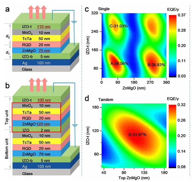
Yuan Figure 2a-d — single- and tandem-QLED stacks beside their calculated cavity-thickness maps. (Source: Yuan et al., Nano Letters 24, 7541–7547 (2024), Figure 2a-d)
Panels a-b identify the two cavities; panel c places the single-layer maximum at 36.56%, while panel d places the tandem maximum at 31.87% and shifts the high-value region to the top-unit cavity dimensions.
Background
Section titled “Background”Top-emitting QLEDs form a microcavity between a semitransparent IZO electrode and an Ag mirror. Changing either the electron-transport-layer thickness or the top-electrode thickness changes the optical phase, field distribution, and fraction of generated light that reaches air. A tandem device adds a second emitting unit, so a useful cavity must support both source positions across the QD emission band.
The paper reports both optical optimization and device stability. This case reproduces only the optical maps EQE/γ; it does not model drive voltage, interconnecting-layer charge generation, or lifetime.
Mapping the Paper to the TMM Model
Section titled “Mapping the Paper to the TMM Model”Single-emitting-layer device (output side → Ag)
Section titled “Single-emitting-layer device (output side → Ag)”| Layer | Thickness |
|---|---|
| IZO top electrode | nominal 110 nm; swept 40–320 nm |
| MoO₃ | 10 nm |
| TCTA | 50 nm |
| Red-QD EML | 20 nm |
| ZnMgO | nominal 70 nm; swept 5–360 nm |
| IZO bottom | 5 nm |
| Ag mirror | 100 nm |
Tandem device (output side → Ag)
Section titled “Tandem device (output side → Ag)”| Layer | Thickness |
|---|---|
| IZO top electrode | nominal 100 nm; swept 20–180 nm |
| Top MoO₃ / TCTA / red-QD EML | 10 / 50 / 20 nm |
| Top ZnMgO | nominal 120 nm; swept 40–180 nm |
| IZO interconnect | 2 nm |
| Bottom MoO₃ / TCTA / red-QD EML | 10 / 50 / 20 nm |
| Bottom ZnMgO | 70 nm |
| IZO bottom | 5 nm |
| Ag mirror | 100 nm |
Both red-QD layers use the same digitized PL spectrum. This reproduction interprets the digitized PL ordinate as a photon-probability spectrum. The source plot does not state its spectral unit; if it represents radiant power instead, it must first be converted by photon energy and the weighted result can change.
The paper combines the two active-unit contributions as
$$ \frac{EQE_{\mathrm{tandem}}}{\gamma_{\mathrm{tandem}}} = \frac{1}{2}\left( \frac{EQE_{b}}{\gamma_{b}}+ \frac{EQE_{t}}{\gamma_{t}} \right). $$
Here, $EQE_{\mathrm{tandem}}$, $EQE_b$, and $EQE_t$ are the external quantum efficiencies of the tandem device, bottom emitting unit, and top emitting unit. The corresponding $\gamma_{\mathrm{tandem}}$, $\gamma_b$, and $\gamma_t$ are their electrical or charge-balance efficiencies. Subscripts $b$ and $t$ denote the bottom and top units. The factor $1/2$ follows the paper’s assumption that the two units have equal charge balance and that $\gamma_b=\gamma_t=\gamma_{\mathrm{tandem}}/2$. The equal-weight two-emitter setting implements this average directly.
With q₀ = 0.9 and the paper’s comparison after dividing out $\gamma$, Mode Top Outcoupling maps to “effective radiative yield × top-outcoupled fraction” and is used as the optical $EQE/\gamma$ quantity. It is neither pure LEE nor a measured EQE because the device’s actual charge balance is not included.
Reproduction Target and Acceptance Criteria
Section titled “Reproduction Target and Acceptance Criteria”- The single-emitting-layer map must place its strongest region near
70–80 nmZnMgO and about110 nmtop IZO. - Its peak must agree with the paper’s
36.56%anchor within one percentage point. - The tandem map must place its strongest region near
110–120 nmtop ZnMgO and100–110 nmtop IZO. - Its peak must agree with the paper’s approximately
31.87%anchor within one percentage point. - Every grid point must complete without a solver error; missing cells would make the optimum comparison ambiguous.
Modeling Path in Dreapex TMM
Section titled “Modeling Path in Dreapex TMM”Structure
Section titled “Structure”Import the corresponding model. The 100 nm Ag mirror is optically thick, so glass behind it is omitted from the emission calculation.
Optical settings
Section titled “Optical settings”Enable Mode and choose spectrum-weighted averaging. The table below records the emitter, wavelength, and sweep settings.
Example Setup
Section titled “Example Setup”Single-emitting-layer model
Section titled “Single-emitting-layer model”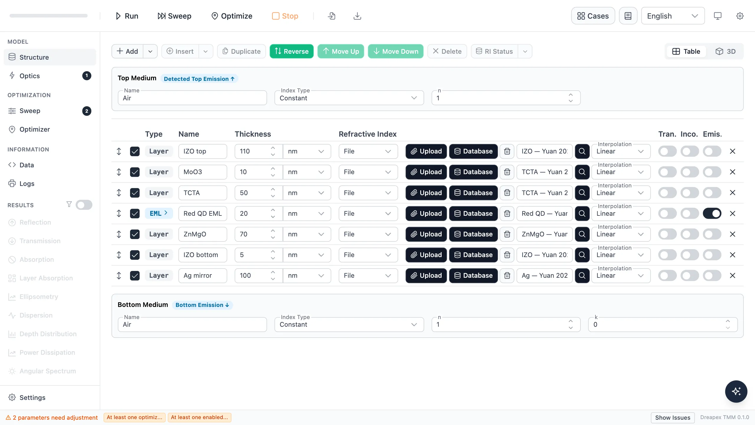
The two swept layers sit on opposite sides of the QD source and jointly tune the cavity phase.

Both QD layers in the tandem model reuse this emitter setting; only the second source position is added.
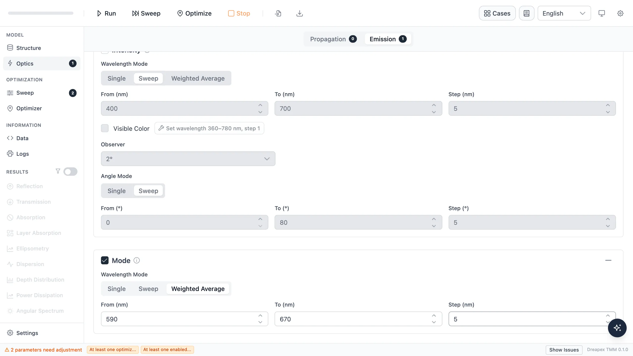
Weighted Average includes the QD PL weight in every thickness combination’s Mode result.
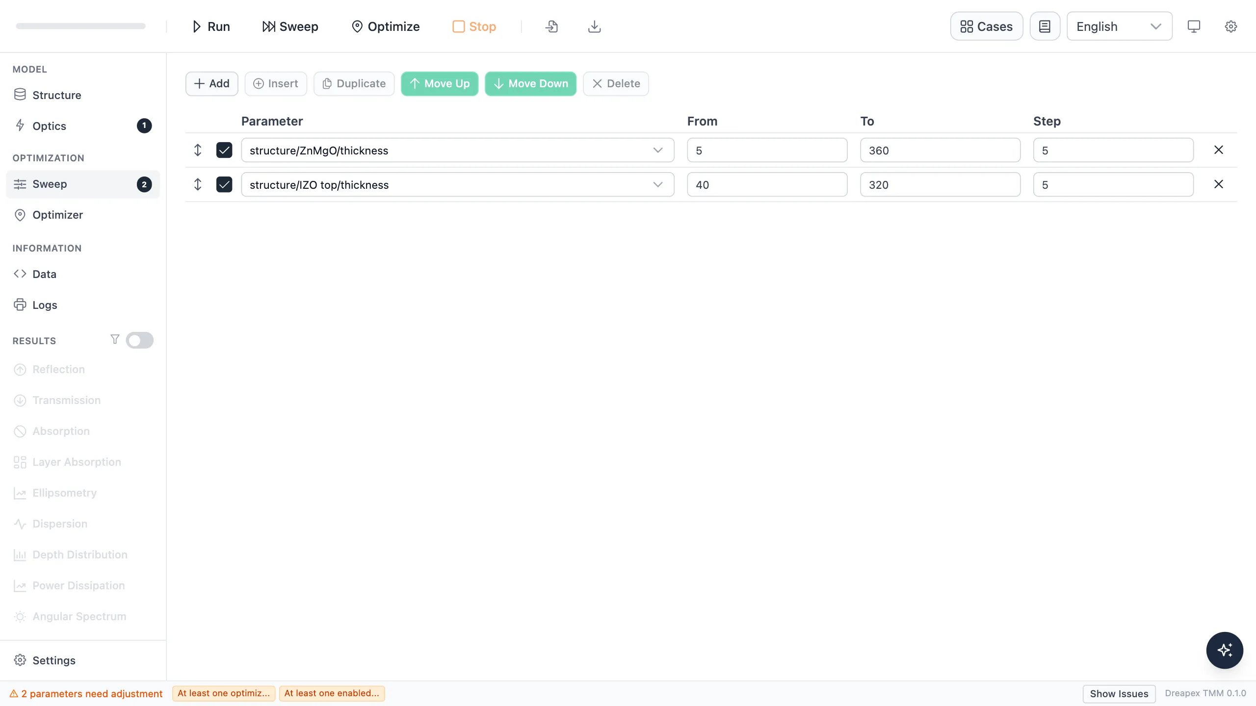
This sweep produces the single-emitter cavity map compared with Figure 2c.
Tandem model
Section titled “Tandem model”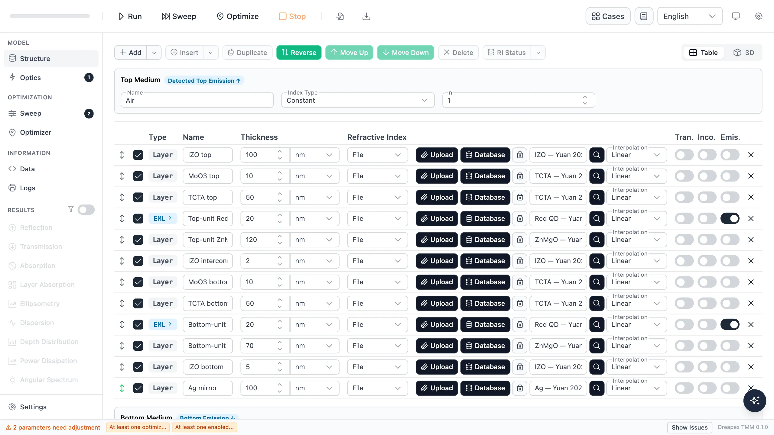
The two QD sources lie on opposite sides of the IZO interconnect and occupy different cavity positions.

The bottom unit uses the same setting and is not shown again.
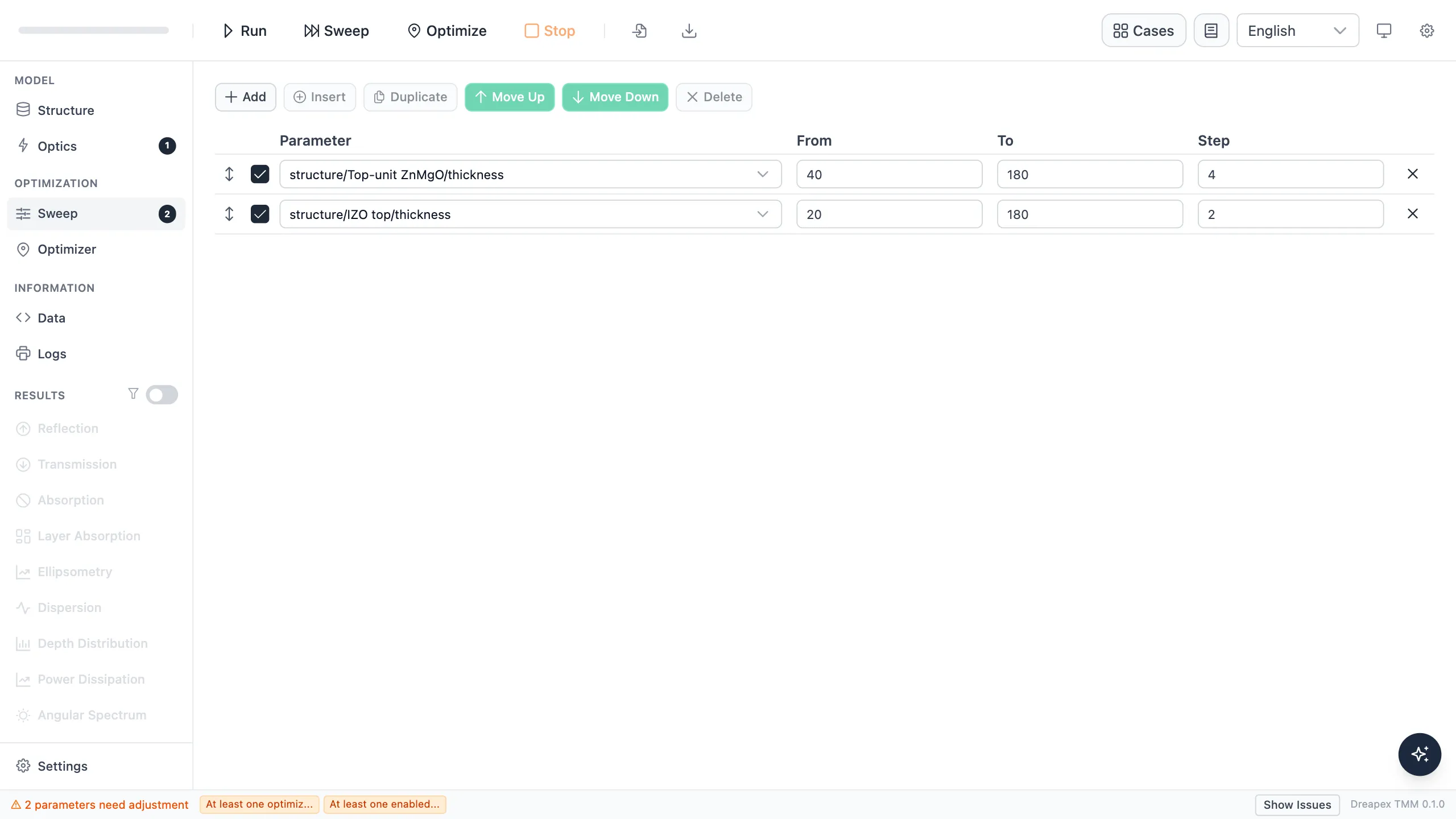
This sweep produces the tandem cavity map compared with Figure 2d.
| Setting | Single-emitting-layer model | Tandem model |
|---|---|---|
| Enabled EMLs | One red-QD EML | Two red-QD EMLs, each with weight 1 |
| Emitters | Digitized PL; Probability; Isotropic; Delta at relative position 0.5; quantum efficiency 0.9 |
Same as the single-layer model |
| Mode | Weighted Average; 590–670 nm; step 5 nm; Top Outcoupling |
Same as the single-layer model |
| Horizontal axis | ZnMgO: 5–360 nm, step 5 nm |
Top ZnMgO: 40–180 nm, step 4 nm |
| Vertical axis | Top IZO: 40–320 nm, step 5 nm |
Top IZO: 20–180 nm, step 2 nm |
| Grid | 72 × 57 = 4,104 combinations |
36 × 81 = 2,916 combinations |
Simulation Results and Comparison with Figure 2
Section titled “Simulation Results and Comparison with Figure 2”Panels c-d use the same color-map logic for the single and tandem devices, allowing the peak values and high-value regions to be compared directly.
Yuan Figure 2a-d — single- and tandem-QLED stacks beside their calculated cavity-thickness maps. (Source: Yuan et al., Nano Letters 24, 7541–7547 (2024), Figure 2a-d)
Figure 2c: single-emitting-layer cavity map
Section titled “Figure 2c: single-emitting-layer cavity map”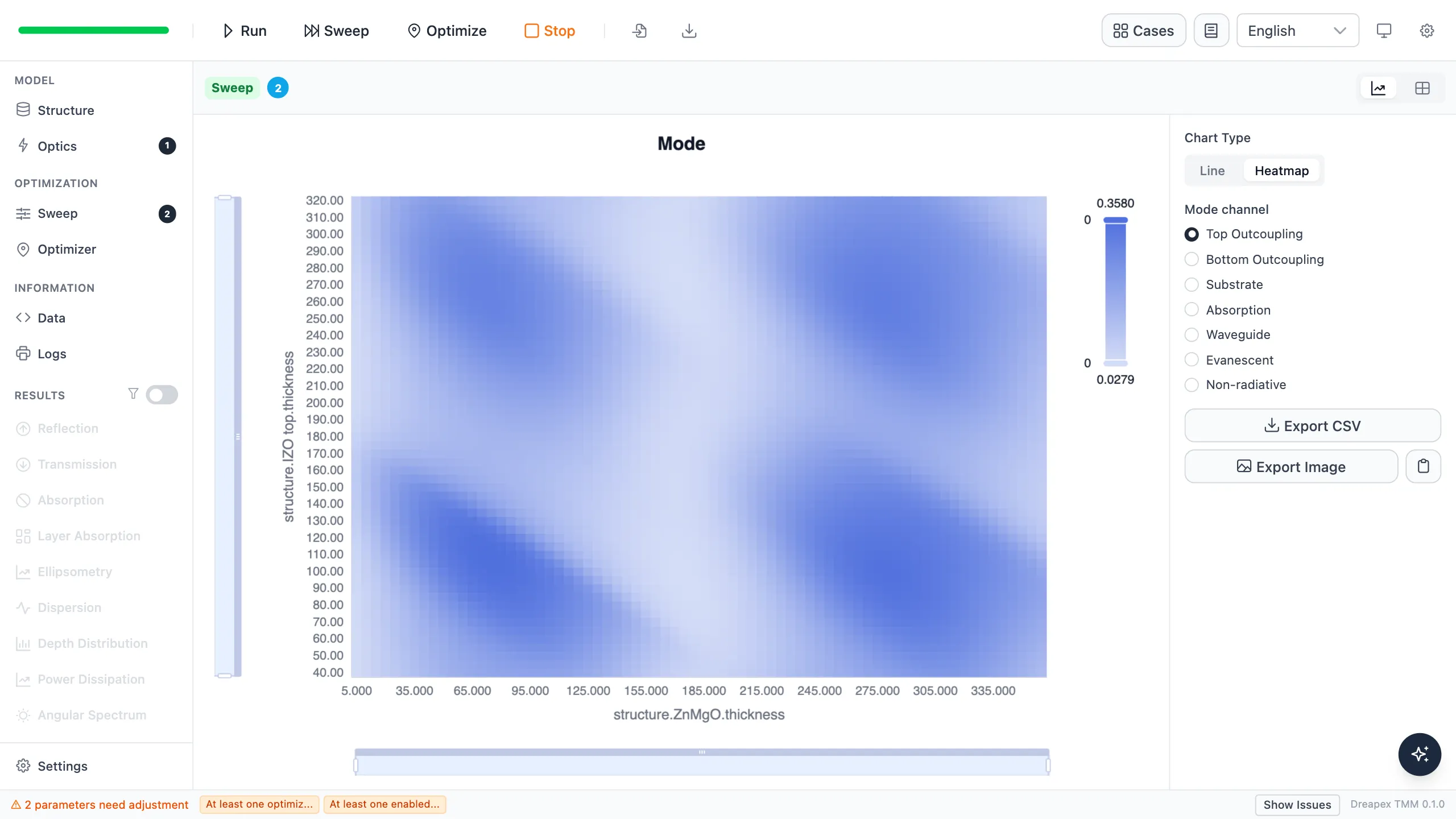
High values form curved bands across both thickness axes, showing that ZnMgO and top IZO compensate cavity phase together. All 4,104 points completed without errors. The maximum is 35.80% at 75 nm ZnMgO and 110 nm top IZO. The paper’s strongest region is centered on the same nominal cavity and reaches 36.56%, a difference of 0.76 percentage point.
Figure 2d: tandem cavity map
Section titled “Figure 2d: tandem cavity map”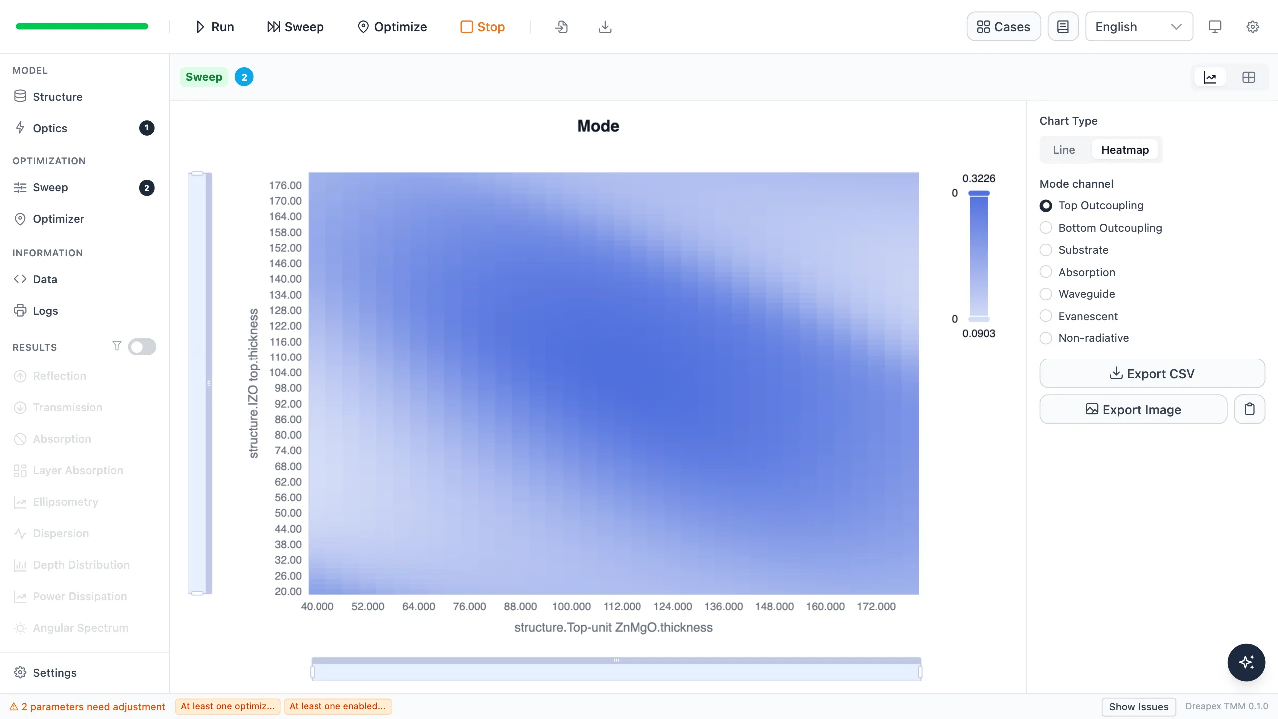
This reproduction uses 4 nm steps for top ZnMgO and 2 nm steps for top IZO so the complete result remains renderable in the browser chart. The main ridge is centered around 112–120 nm top ZnMgO and 100–106 nm top IZO and extends diagonally along both axes, showing that the two thicknesses compensate cavity phase together. All 2,916 points completed without errors. The maximum is 31.87% at 112/106 nm; the paper’s nominal 120/100 nm design gives 31.72%, only 0.14 percentage point below the maximum.
| Quantity | Paper | Simulation |
|---|---|---|
| Single-device peak | 36.56% |
35.80% |
| Single optimum | near 70/110 nm |
75/110 nm |
| Tandem peak | about 31.87% |
31.87% |
| Tandem optimum | near 120/100 nm |
112/106 nm |
The single-device result closely reproduces the peak magnitude and design region. The tandem peak magnitude is effectively identical on the reported precision; its optimum sits 8 nm lower in top ZnMgO and 6 nm higher in top IZO than the nominal paper design.
Deviation Analysis
Section titled “Deviation Analysis”- The Supporting Information plots provide refractive index but not extinction coefficient for RQD and TCTA; their
kvalues are explicitly set to zero. - MoO₃ reuses the TCTA optical constants, following the approximation stated in the Supporting Information rather than an independent MoO₃ dataset.
- The PL and optical-constant curves are digitized. Sampling and interpolation can move a narrow cavity optimum by several nanometres.
- Each EML is represented by one central isotropic delta emitter. A distributed recombination zone or unequal unit weights would reshape the tandem map.
- The planar model excludes electrode roughness and scattering. It predicts the optical
EQE/γmap, not the measured device EQE or lifetime.
Further Extensions
Section titled “Further Extensions”- Run a
1 nmlocal sweep around the two maxima to estimate the continuous optimum. - Replace the TCTA-based MoO₃ approximation with measured complex dispersion.
- Sweep the relative weights of the two tandem emitters to represent electrical imbalance.
- Add emitter-position variables to quantify the tolerance of both recombination zones.
Going further
Section titled “Going further”These tutorials cover the operating steps only. The physics behind them, the full parameter reference for each feature, how to read the results, and the algorithm validation all live on the documentation site:
- Transfer-Matrix Method — the physics and formulas behind these tutorials
- Feature Guide — complete reference for every screen and parameter
- Results — how to read each kind of output
- Open Dreapex TMM — build and simulate in the browser