Regular Tandem QLED Outcoupling
Author: Zhengqi ZHANG
Regular Tandem Quantum Dot Light-Emitting Diodes with over 51% External Quantum Efficiency for Next-Generation Displays Authors: Dawei Yang, Yiduo Wang, Jing Xie, Daocheng Pan, Bingsuo Zou, and Heng Zhang Journal: Advanced Materials 37(44), e08173 (2025) · Comparison target: Figure 2i-k https://doi.org/10.1002/adma.202508173
This case reproduces the 632 nm optical analysis in Figure 2i-k of Yang et al. The bottom-unit ZnMgO thickness is swept from 22 to 200 nm for the bottom emitter, top emitter, and equal-weight tandem model. The calculation reproduces the larger top-unit contribution and the broad cavity optima, while underestimating the paper’s summed outcoupling at its 120 nm design point.
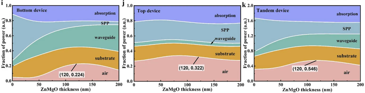
Yang Figure 2i-k — calculated power fractions of the bottom unit, top unit, and tandem device as bottom-unit ZnMgO thickness changes. (Source: Yang et al., Advanced Materials (2025), Figure 2i-k)
At 120 nm, the paper marks Air fractions of 22.4% for the bottom unit, 32.2% for the top unit, and 54.6% for their summed tandem contribution. The broad maxima and the larger top-unit contribution are the main comparison features.
Background
Section titled “Background”A tandem QLED places two emissive units in one optical stack. Under ideal charge balance, one injected electron can generate at most one exciton in each unit. Optically, the two QD layers occupy different positions relative to the output interface and metal cathode, so their outcoupling efficiencies are not equal and respond differently to the same transport-layer thickness.
The paper uses an ultrathin ITO charge-generation layer and reports an experimental EQE above 51%. This reproduction addresses the optical power fractions only. Charge generation, carrier balance, and lifetime are outside the model.
Mapping the Paper to the TMM Model
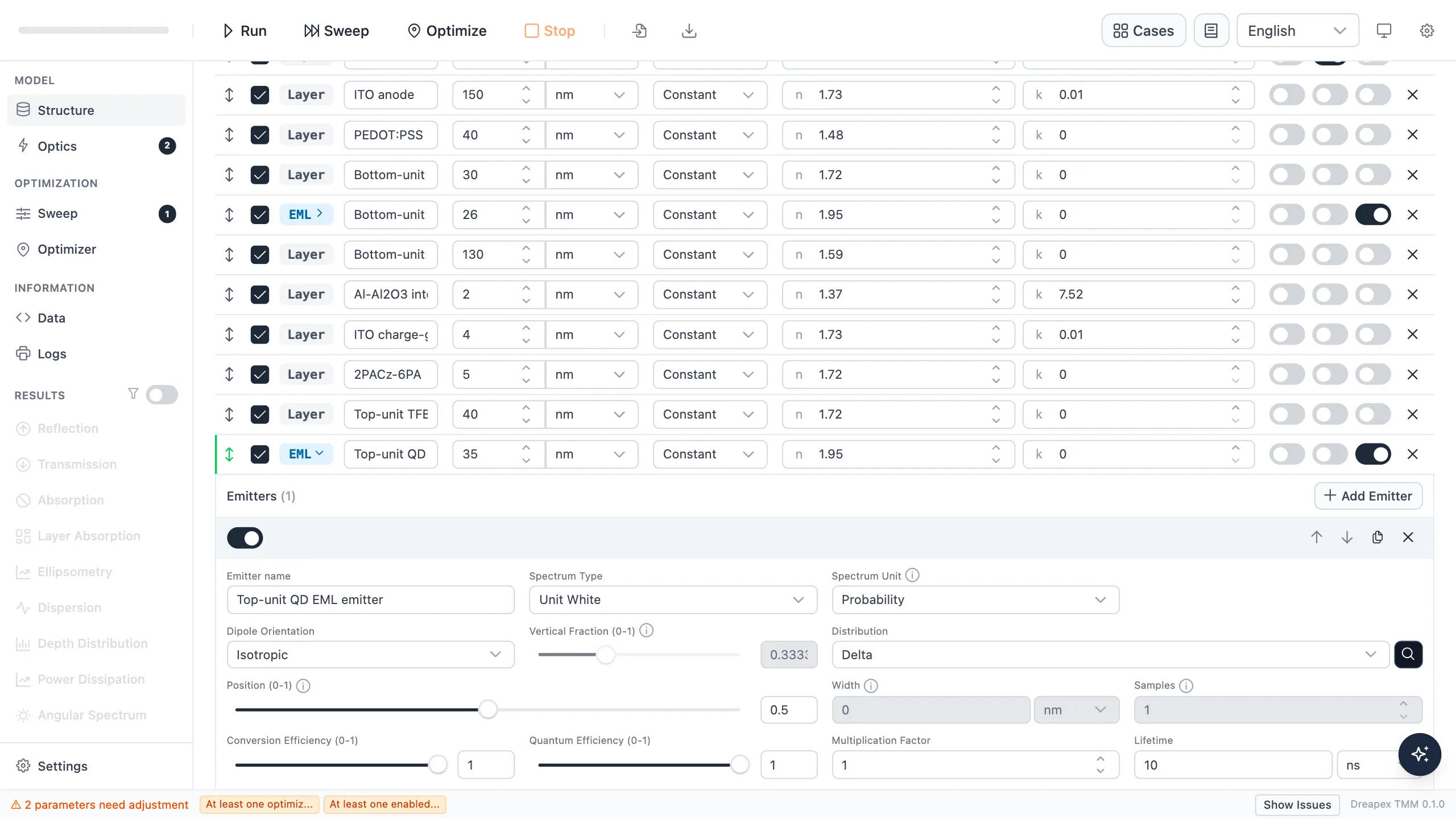
Section titled “Mapping the Paper to the TMM Model”Complete stack (Glass output side → Al cathode)
Section titled “Complete stack (Glass output side → Al cathode)”| Layer | Thickness | Optical constant at 632 nm |
|---|---|---|
| Glass, incoherent | 1 mm |
substrate model |
| ITO anode | 150 nm |
1.73 + 0.01i |
| PEDOT:PSS | 40 nm |
1.48 |
| Bottom TFB | 30 nm |
1.72 |
| Bottom QD EML | 26 nm |
1.95 |
| Bottom ZnMgO | nominal 130 nm; swept |
1.59 |
| Al–Al₂O₃ interconnect | 2 nm |
1.37 + 7.52i |
| ITO charge-generation layer | 4 nm |
1.73 + 0.01i |
| 2PACz:6PA | 5 nm |
1.72 |
| Top TFB | 40 nm |
1.72 |
| Top QD EML | 35 nm |
1.95 |
| Top ZnMgO | 50 nm |
1.59 |
| Al cathode | 110 nm |
1.37 + 7.52i |
Reproduction Target and Acceptance Criteria
Section titled “Reproduction Target and Acceptance Criteria”- Around
120 nmbottom ZnMgO, the top-unit outcoupling must exceed the bottom-unit outcoupling. - All three thickness responses must be smooth and exhibit a cavity optimum rather than a monotonic trend.
- The bottom- and top-unit curves must peak at different thicknesses, confirming that the two emitters occupy different optical positions.
- The paper’s summed
54.6%value must be compared with the sum of the two isolated-unit simulations. The dual-emitter Mode trace displays the average of two equal-weight inputs and is retained only as a thickness-trend check, not as device EQE.
This is a trend-level acceptance test. Exact agreement at 120 nm is not required because two optical layers use scalar effective-index approximations.
Modeling Path in Dreapex TMM
Section titled “Modeling Path in Dreapex TMM”Structure
Section titled “Structure”The three models share the stack above and differ only in which QD layers have Emission enabled.
Optical settings
Section titled “Optical settings”Enable Mode and use Top Outcoupling as the comparison channel. The table below records the wavelength, emitter, and sweep settings.
Example Setup
Section titled “Example Setup”Complete stack
Section titled “Complete stack”
The two QD layers sit on opposite sides of the interconnect and share the Glass output channel.
Emitters
Section titled “Emitters”
The bottom-unit model enables only this emitter.
The top-unit model enables only this emitter; the tandem model enables both.
Mode and sweep
Section titled “Mode and sweep”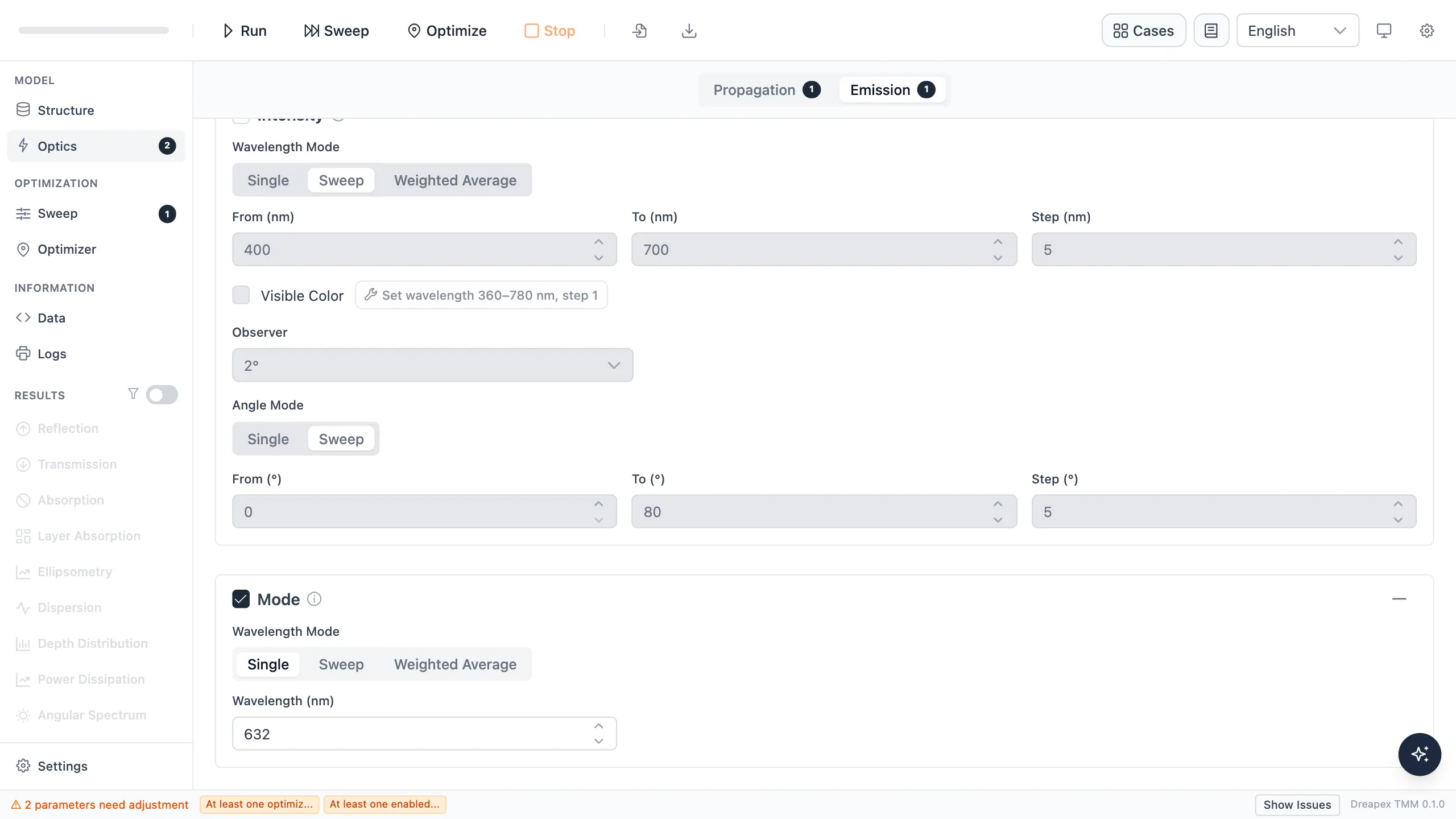
Only the Top Outcoupling channel is used for the numerical comparison.

All three models use the same 90 thickness values, so their curves are directly comparable.
| Setting | Value |
|---|---|
| Bottom-unit model | Only the bottom QD EML enabled |
| Top-unit model | Only the top QD EML enabled |
| Tandem model | Both QD EMLs enabled with equal weight |
| Emitters | Unit White; Probability; Isotropic; Delta at relative position 0.5; quantum efficiency 1 |
| Mode | Single, 632 nm, Top Outcoupling |
| Sweep | Bottom-unit ZnMgO: 22–200 nm, step 2 nm, 90 values |
In this case, Unit White means that the single-wavelength calculation uses no additional PL weighting; it does not indicate white device emission.
Simulation Results and Comparison with Figure 2
Section titled “Simulation Results and Comparison with Figure 2”The paper separates the bottom, top, and summed tandem power fractions, so the simulation results follow the same i-j-k order.
Yang Figure 2i-k — calculated power fractions of the bottom unit, top unit, and tandem device as bottom-unit ZnMgO thickness changes. (Source: Yang et al., Advanced Materials (2025), Figure 2i-k)
Figure 2i: bottom unit
Section titled “Figure 2i: bottom unit”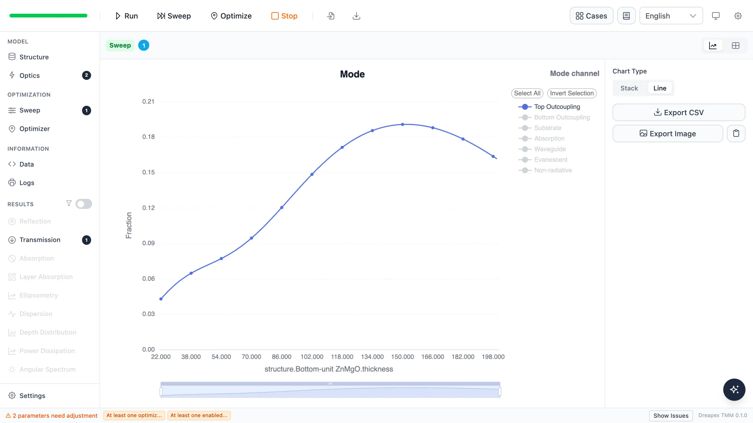
The bottom unit gives 17.35% at 120 nm and reaches 19.07% near 152 nm; the paper reports about 22.4% at 120 nm. The broad cavity optimum is reproduced, with visible offsets in both position and magnitude.
Figure 2j: top unit
Section titled “Figure 2j: top unit”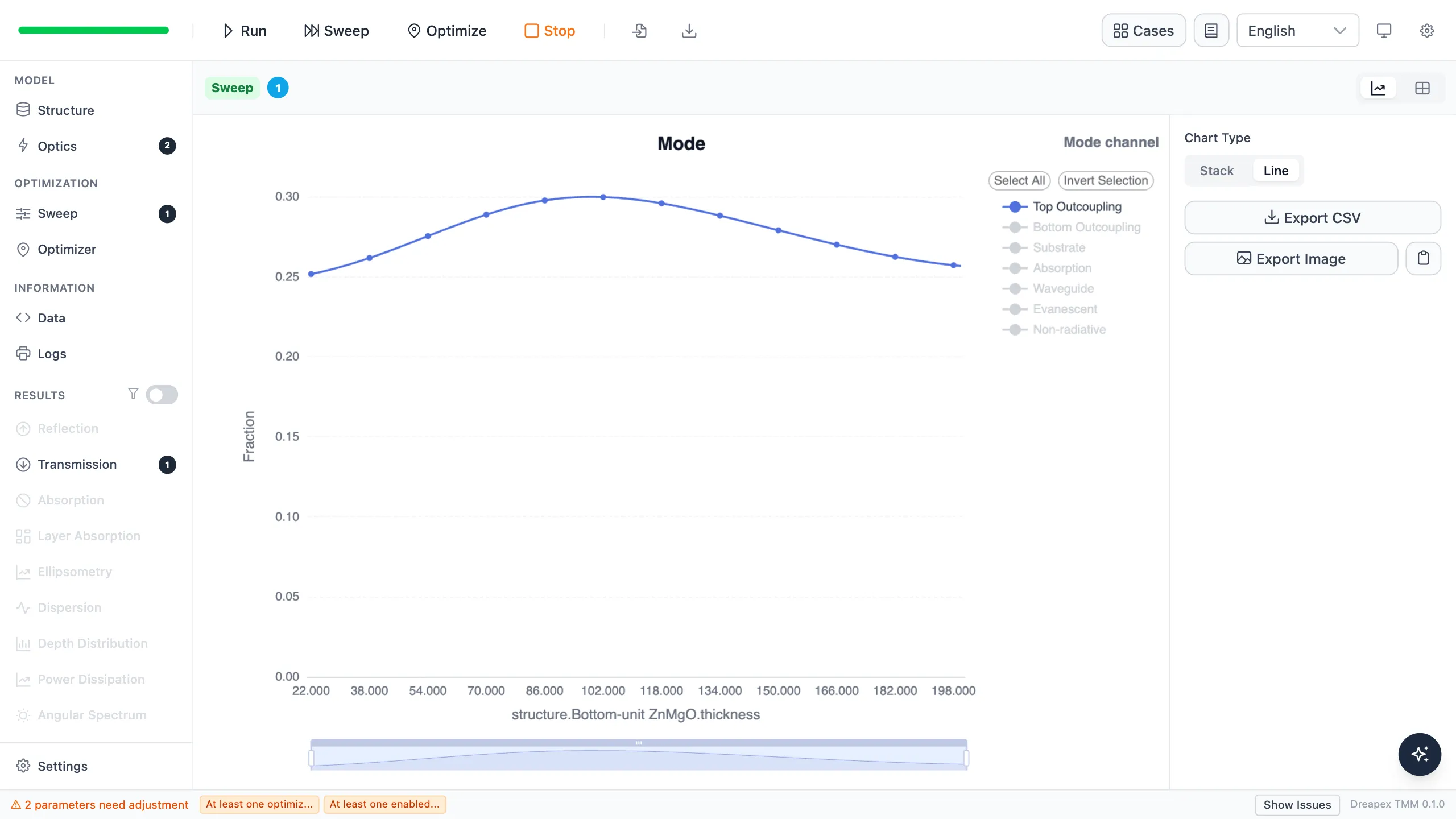
The top unit gives 29.49% at 120 nm and peaks at 29.98% near 98 nm. Its optimum differs from the bottom unit’s 152 nm, showing that the two QD layers occupy different optical positions. The contribution ordering at the design point agrees with the paper’s 32.2% > 22.4%.
Figure 2k: tandem device
Section titled “Figure 2k: tandem device”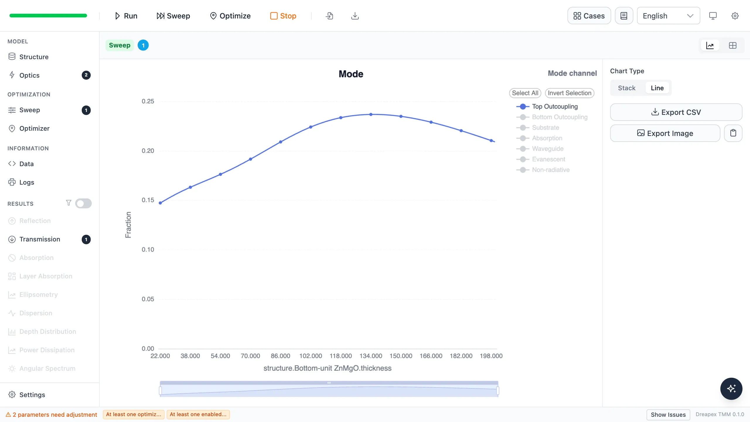
The dual-emitter trace is the equal-weight average of the two Top Outcoupling results, not the sum of the isolated contributions in Figure 2k or the device EQE. It reaches 23.68% near 136 nm, gives 23.42% at the paper’s 120 nm design, and remains between the two isolated traces.
Quantity at 120 nm |
Paper | Simulation |
|---|---|---|
| Bottom-unit contribution | 22.4% |
17.35% |
| Top-unit contribution | 32.2% |
29.49% |
| Sum of isolated units | 54.6% |
46.84% |
| Equal-weight dual-emitter Mode average | trend check only | 23.42% |
The quantitative Figure 2k comparison uses the isolated-unit sum: 17.35% + 29.49% = 46.84%, which is 7.76 percentage points below the paper’s 54.6%. At 120 nm, the dual-emitter 23.42% agrees with the arithmetic mean of the isolated results; it verifies equal-weight combination and the broad optimum, but is excluded from the 54.6% error calculation.
Deviation Analysis
Section titled “Deviation Analysis”- The
2 nmAl–Al₂O₃ interconnect uses the paper’s single effective value1.37 + 7.52i. Treating a mixed ultrathin layer as one strongly absorbing homogeneous film can change both the bottom-unit loss and optimum position. - The 2PACz:6PA layer uses the scalar
1.72surrogate reported for the optical calculation; dispersion and absorption are not available. - Each QD layer uses a central isotropic delta emitter. Different recombination-zone positions or horizontal-dipole fractions would affect the two units differently.
- The model excludes electrical charge balance. The experimental
51.2%EQE is therefore not a direct optical acceptance target.
Further Extensions
Section titled “Further Extensions”- Replace the interconnect effective index with measured complex dispersion and repeat all three sweeps.
- Sweep bottom ZnMgO and the emitter position together to separate cavity-phase and recombination-zone effects.
- Assign measured spectra to the two QD units and run spectrum-weighted Mode calculations.
- Compare equal and unequal emitter weights to represent current imbalance between the two units.
Back to Case Studies · Next: Tandem QLED Cavity Optimization
Going further
Section titled “Going further”These tutorials cover the operating steps only. The physics behind them, the full parameter reference for each feature, how to read the results, and the algorithm validation all live on the documentation site:
- Transfer-Matrix Method — the physics and formulas behind these tutorials
- Feature Guide — complete reference for every screen and parameter
- Results — how to read each kind of output
- Open Dreapex TMM — build and simulate in the browser