Top-Emitting QLED Outcoupling
Highly Efficient Top-Emitting Quantum-Dot Light-Emitting Diodes with Record-Breaking External Quantum Efficiency of over 44.5% Authors: Haotao Li, Shiming Zhou, and Shuming Chen Journal: Laser & Photonics Reviews 17(8), 2300371 (2023) · Comparison target: Figures 1b-d, 3c, 3f, 4a, and 4c https://doi.org/10.1002/lpor.202300371
Li et al. (2023) compared optical losses in bottom- and top-emitting red QLEDs and used two IZO layers to tune the microcavity phase in the top-emitting device. The thicknesses of these layers determine the power partition among optical modes and the fraction of emission that escapes through the top surface.
These figures form the optical argument of the paper. EQE/γ is the external quantum efficiency normalized by the charge-balance factor γ, which isolates the contribution of the optical structure.
| Paper figure | Role in the paper | Calculation reproduced in this case |
|---|---|---|
| Figure 1b | Quantifies the outcoupled, substrate, waveguide, surface-plasmon-polariton (SPP), and absorption channels in bottom- and top-emitting devices | Mode results for both structures at 626 nm |
| Figure 1c | Locates substrate-, waveguide-, and SPP-mode features on the in-plane-wavevector axis and explains the change in mode partition | Power Dissipation results for both structures at 626 nm |
| Figure 1d | Maps the high-efficiency region and optimum defined jointly by the two IZO thicknesses | Two-variable IZO thickness sweep and the maximum EQE/γ |
| Figure 3c | Tests the periodic modulation of wide-angle interference and EQE/γ by the bottom IZO layer | Bottom-IZO sweep at fixed top-IZO thickness |
| Figure 3f | Tests the modulation of multiple-beam interference by the top IZO layer and identifies the combined IZO thicknesses | Top-IZO sweep at fixed bottom-IZO thickness |
| Figure 4a | Shows how increasing bottom-IZO thickness transfers power among outcoupled, waveguide, SPP, and other channels | Mode fractions versus bottom-IZO thickness |
| Figure 4c | Uses peak shifts and the number of waveguide modes to explain Figure 4a and motivate subsequent waveguide extraction | Power-dissipation spectra for 0, 5, and 160 nm bottom IZO |
This case follows that sequence to reproduce Figures 1b-d, 3c, 3f, 4a, and 4c, with a point-by-point comparison between the published values and real Dreapex TMM calculations.
Reproduction Data
Section titled “Reproduction Data”Download the refractive-index and emission-spectrum files before building the models. The refractive-index data were extracted from Figure S1 of the paper’s supporting information. Cite Li et al. (2023) when reusing these files.
Refractive-index data
Section titled “Refractive-index data”| Material | Download |
|---|---|
| IZO | :case-data-download{path="/data/case-studies/top-emitting-qled-outcoupling/IZO1-lpor.202300371.nk"} |
| PEDOT:PSS | :case-data-download{path="/data/case-studies/top-emitting-qled-outcoupling/PEDOT-lpor.202300371.nk"} |
| TFB | :case-data-download{path="/data/case-studies/top-emitting-qled-outcoupling/TFB-lpor.202300371.nk"} |
| Red CdSe QD | :case-data-download{path="/data/case-studies/top-emitting-qled-outcoupling/RQD1-lpor.202300371.nk"} |
| ZnMgO | :case-data-download{path="/data/case-studies/top-emitting-qled-outcoupling/ZnMgO-lpor.202300371.nk"} |
| Ag | :case-data-download{path="/data/case-studies/top-emitting-qled-outcoupling/Ag-lpor.202300371.nk"} |
Emission-spectrum data
Section titled “Emission-spectrum data”:case-data-download{path="/data/case-studies/top-emitting-qled-outcoupling/Red%20CdSe%20QD-lpor.202300371.pl" label="Red CdSe QD PL spectrum"}
Structure
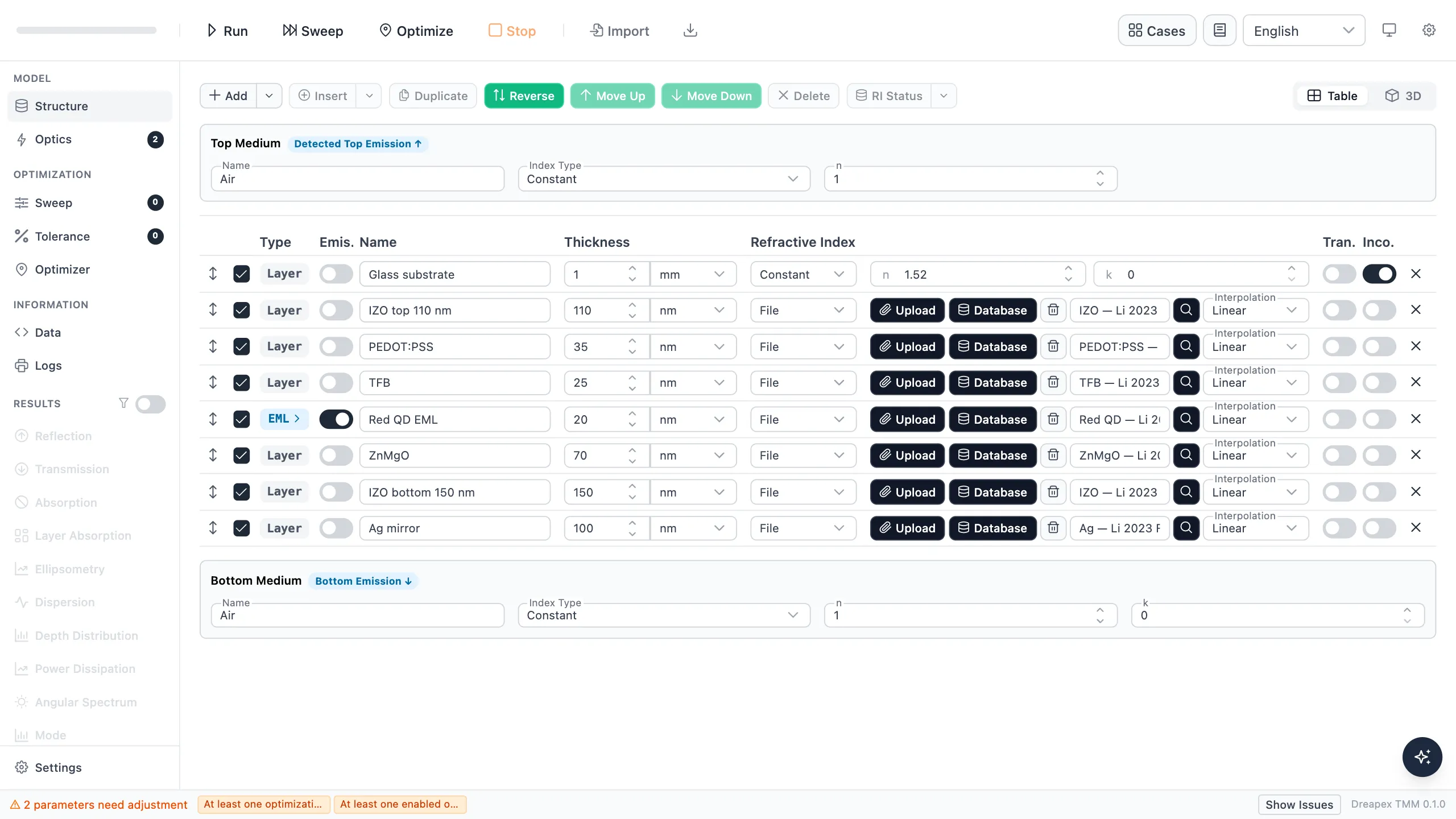
Section titled “Structure”Build the bottom- and top-emitting models using the tables below; see Emission Structure for the setup procedure. Layers are listed from the output side to the Ag reflector. The models exclude the external scattering layer.
Bottom-emitting structure
Section titled “Bottom-emitting structure”The bottom-emitting device emits through the glass substrate. Set Glass as incoherent (Inco.) and the QD layer as emissive (Emis.).
| Layer | Thickness | Layer state |
|---|---|---|
| Glass | 1 mm | Inco. |
| IZO top | 110 nm | None |
| PEDOT:PSS | 35 nm | None |
| TFB | 25 nm | None |
| Red QD EML | 20 nm | Emis. |
| ZnMgO | 70 nm | None |
| IZO bottom | 150 nm | None |
| Ag | 100 nm | None |
The bottom-emitting structure is configured as follows:
Top-emitting structure
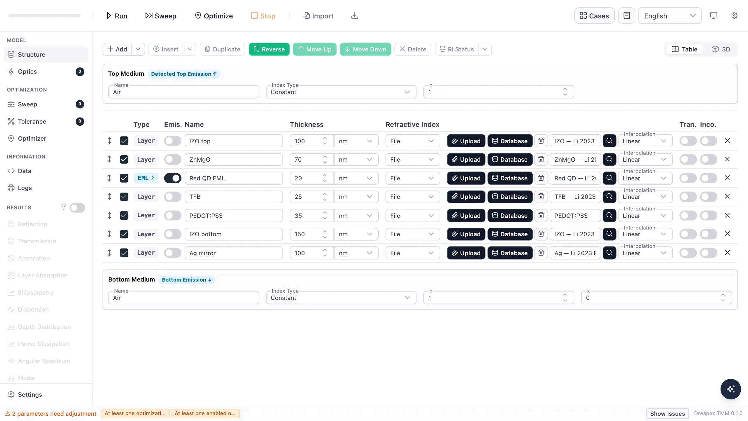
Section titled “Top-emitting structure”The top-emitting device emits through the top IZO electrode. The Mode detector requires every finite layer below the emissive layer to remain coherent, so an incoherent Glass substrate cannot be added after the 100 nm Ag layer. The Ag layer is effectively opaque, so omitting the Glass behind it does not materially change the calculation.
| Layer | Thickness | Layer state |
|---|---|---|
| IZO top | 100 nm | None |
| ZnMgO | 70 nm | None |
| Red QD EML | 20 nm | Emis. |
| TFB | 25 nm | None |
| PEDOT:PSS | 35 nm | None |
| IZO bottom | 150 nm | None |
| Ag | 100 nm | None |
The top-emitting structure is configured as follows:
Optical and Emitter Settings
Section titled “Optical and Emitter Settings”Both structures use the same emitter and detector settings to calculate optical mode partition and power-dissipation spectra at 626 nm.
Emitter
Section titled “Emitter”Expand Emitters in the Red QD EML layer of each structure, add one emitter, and use the settings below. Delta places the dipoles at a single relative position, set here to the centre of the QD layer at 0.5.
| UI field | Setting |
|---|---|
Emitter name |
Red QD PL |
Spectrum Type |
File |
Spectrum Unit |
Probability |
Spectrum File |
Import Red CdSe QD-lpor.202300371.pl downloaded above |
Dipole Orientation |
Isotropic |
Distribution |
Delta |
Position |
0.5 |
Conversion Efficiency |
1 |
Quantum Efficiency |
1 |
Multiplication Factor |
1 |
The configured emitter is shown below:

Mode detector
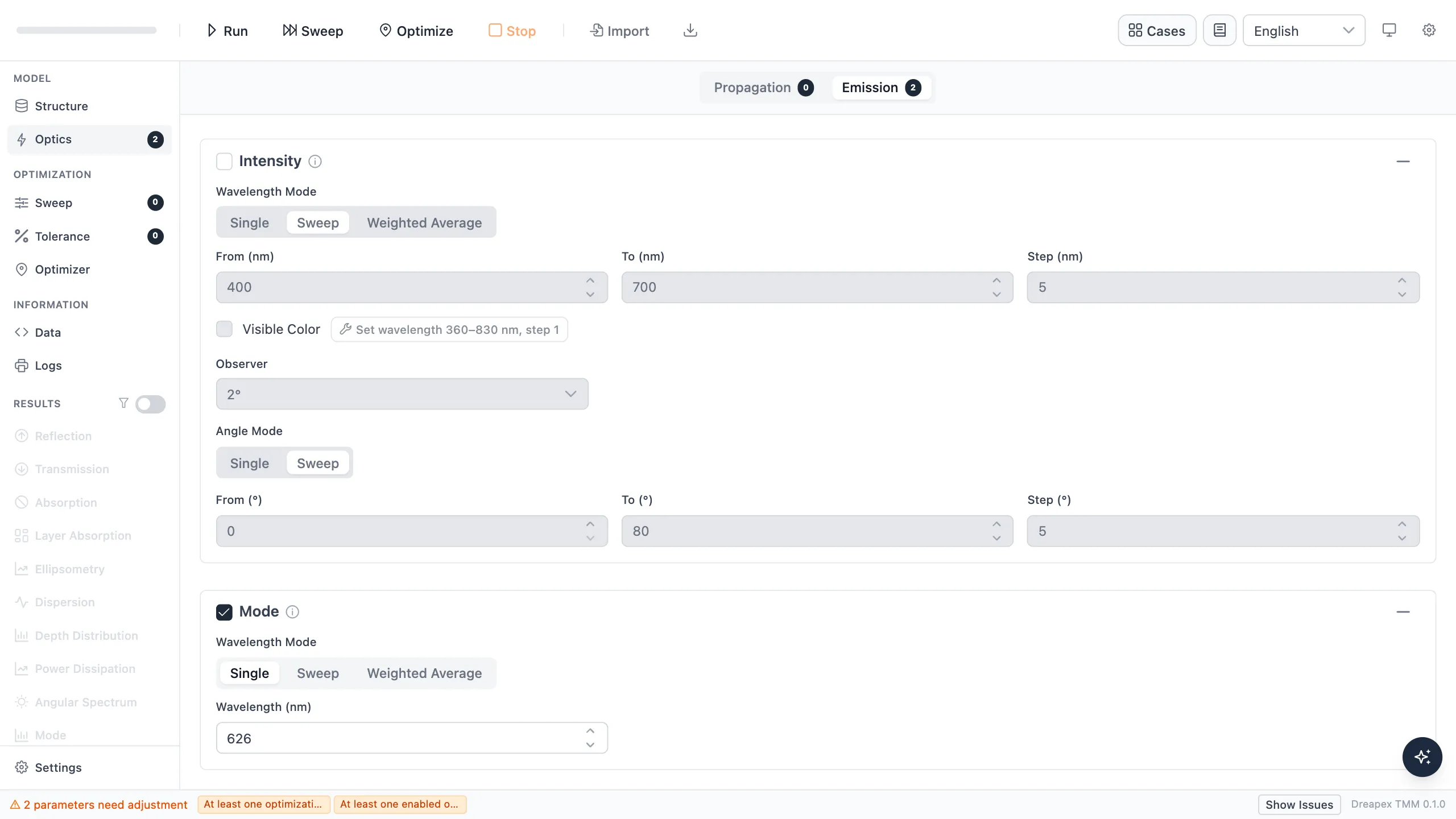
Section titled “Mode detector”Open the Emission page under Optics and enable Mode. Set Wavelength Mode to Single and Wavelength to 626 nm. These settings produce the single-wavelength mode fractions required for Figure 1b.
Power Dissipation detector
Section titled “Power Dissipation detector”On the same Emission page, enable Power Dissipation and use the settings below. In-plane u is the normalized in-plane wavevector used on the horizontal axis of paper Figure 1c.
| UI field | Setting |
|---|---|
Wavelength Mode |
Single |
Wavelength |
626 nm |
In-plane Vector Type |
In-plane u |
From |
0 |
To |
2 |
Step |
0.002 |
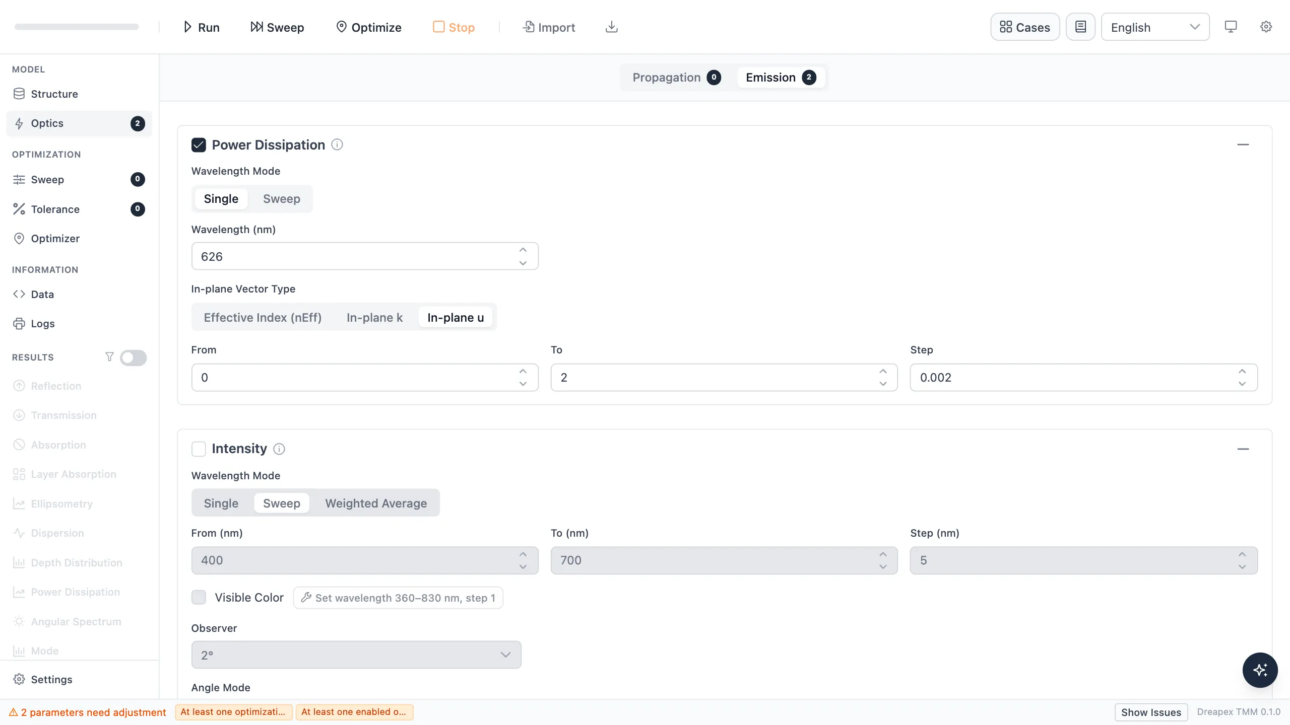
Repeat the same emitter, Mode, and Power Dissipation settings in the top-emitting model. Click Run for each structure.
Bottom- and Top-Emitting Mode Comparison (Figures 1b and 1c)
Section titled “Bottom- and Top-Emitting Mode Comparison (Figures 1b and 1c)”Power Distribution Among Optical Modes (Figure 1b)
Section titled “Power Distribution Among Optical Modes (Figure 1b)”The chart compares the data from paper Figure 1b with Dreapex TMM Mode results by optical channel:
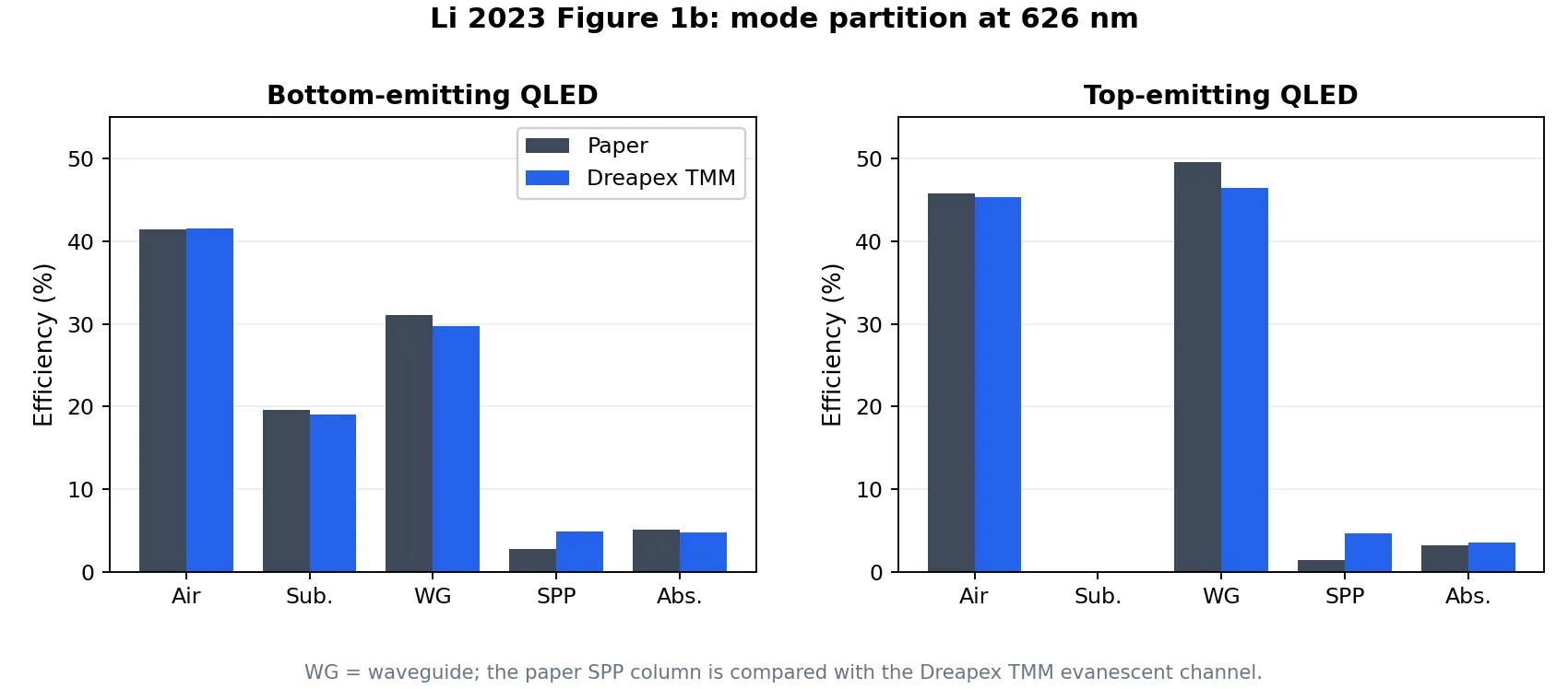
Channel efficiencies from paper Figure 1b beside the 626 nm Mode runs of this case, in the same channel order. (Source: Paper data from Li et al. Figure 1b; Dreapex TMM data from the real runs of this case; graphic by Dreapex)
The emitting side of the top-emitting model has no incoherent substrate, so Substrate is 0. Its Top Outcoupling and Waveguide fractions are both higher than those of the bottom-emitting model.
| Channel | Paper, bottom-emitting | This run, bottom-emitting | Paper, top-emitting | This run, top-emitting |
|---|---|---|---|---|
| Air / Top Outcoupling | 41.42% | 41.53% | 45.74% | 45.32% |
| Sub / Substrate | 19.62% | 19.02% | 0% | 0% |
| WG / Waveguide | 31.05% | 29.78% | 49.54% | 46.42% |
| SPP / Evanescent | 2.80% | 4.87% | 1.47% | 4.65% |
| Abs / Absorption | 5.10% | 4.79% | 3.25% | 3.59% |
The bottom-emitting outcoupling fraction is 0.11 percentage point above the paper value; the top-emitting fraction is 0.42 percentage point below it. Substrate is power coupled into glass that does not escape into air. The difference between the paper’s SPP values and Dreapex TMM’s Evanescent values may result from different in-plane-wavevector ranges.
Power Dissipation over In-Plane Wavevector (Figure 1c)
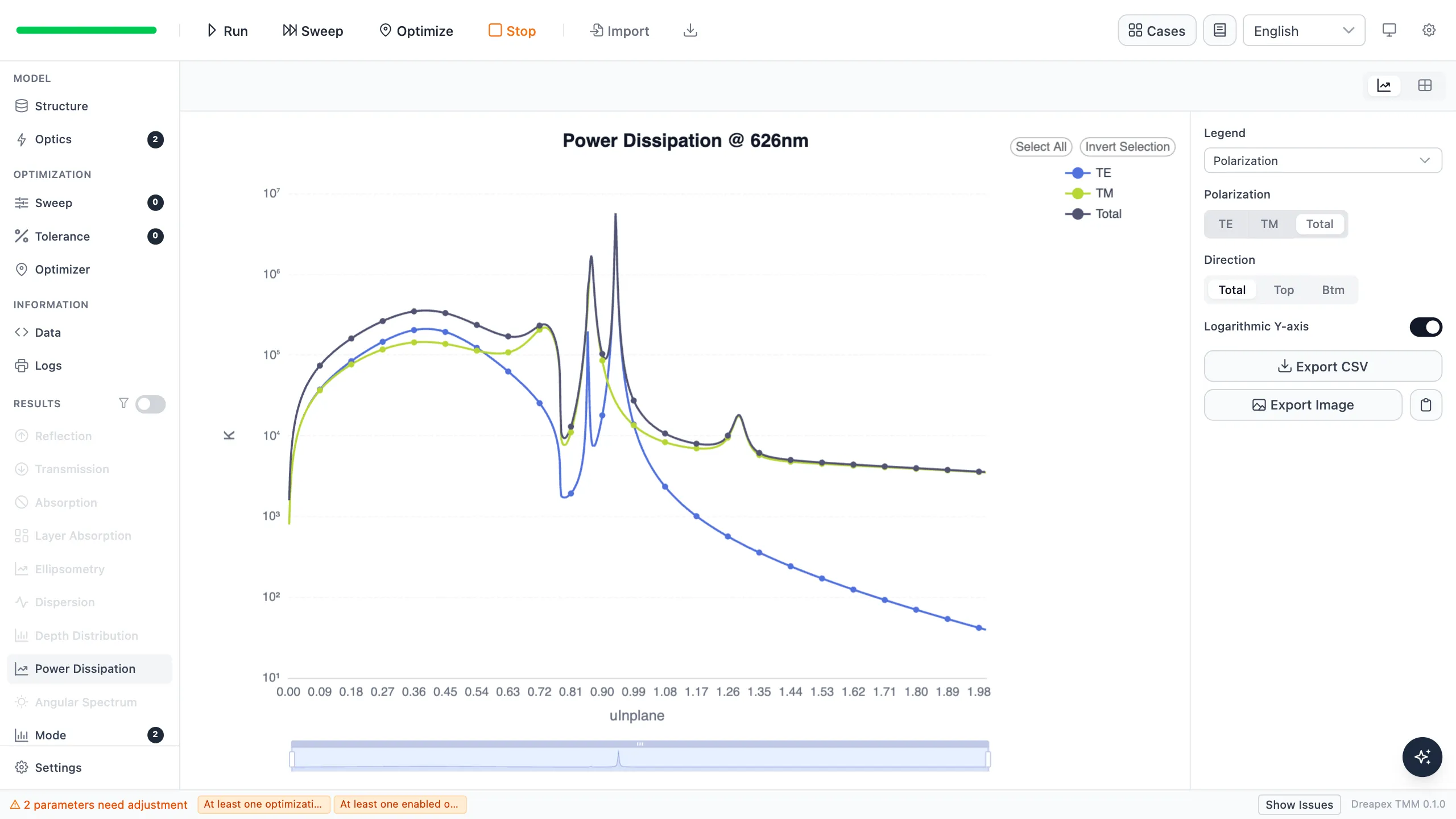
Section titled “Power Dissipation over In-Plane Wavevector (Figure 1c)”Paper Figure 1c compares the power-dissipation spectra of the bottom- and top-emitting structures at 626 nm. Run both models and open the Power Dissipation result. In the right control panel, set Polarization to Total, set Direction to Total, and enable Logarithmic Y-axis. To export the raw data, click Export CSV; the peak positions below use the uInplane and K_total columns.
The bottom-emitting result is shown below:
The top-emitting result is shown below:
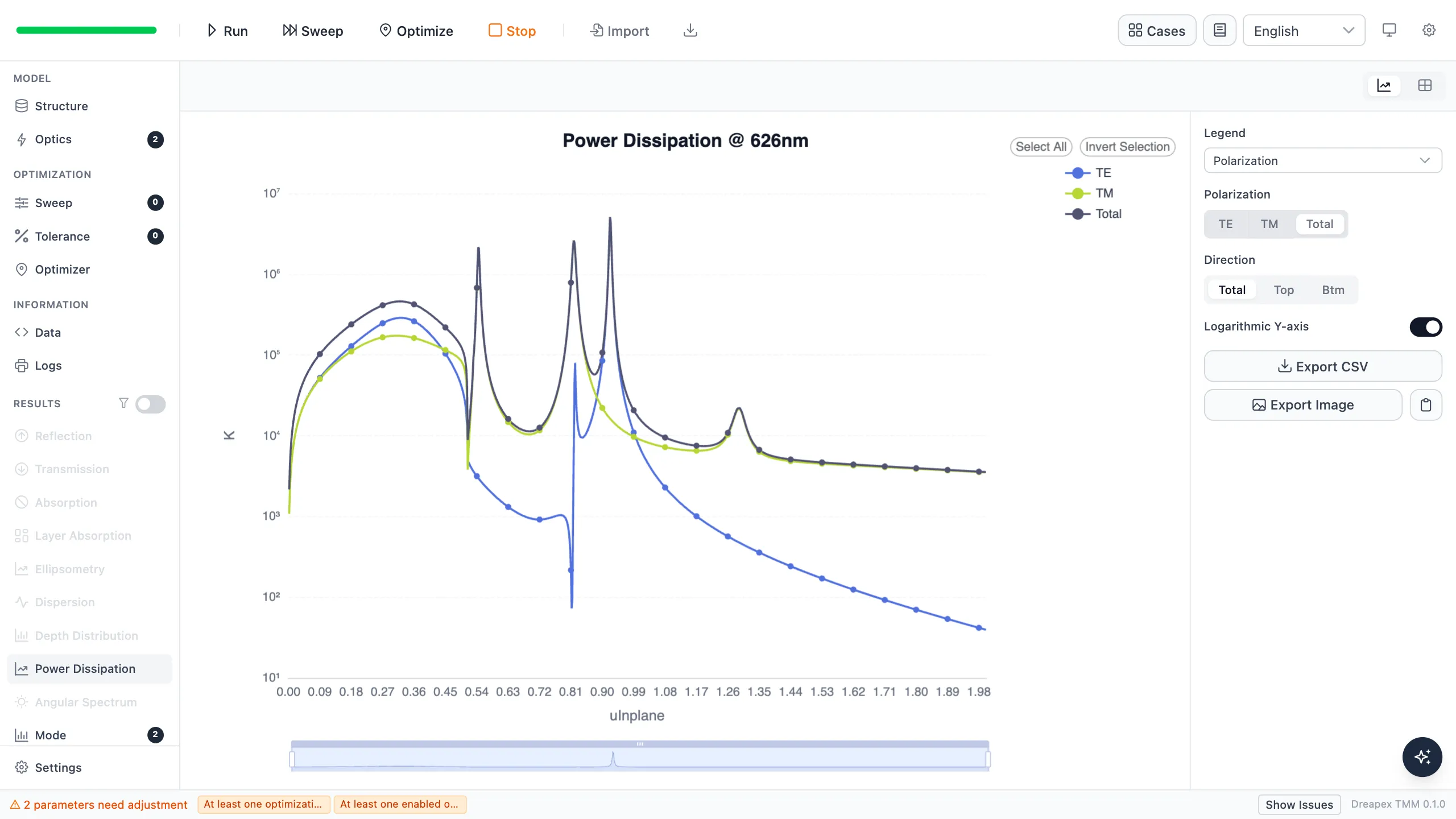
| Structure | Mode feature | Paper $u$ | Simulation $u$ | $\Delta u$ |
|---|---|---|---|---|
| Bottom-emitting | Sub | 0.72 | 0.732 | +0.012 |
| Bottom-emitting | WG1 | about 0.87 | 0.868 | -0.002 |
| Bottom-emitting | WG2 | about 0.96 | 0.938 | -0.022 |
| Top-emitting | WG1 | about 0.55 | 0.544 | -0.006 |
| Top-emitting | WG2 | about 0.82 | 0.818 | -0.002 |
| Top-emitting | WG3 | about 0.94 | 0.922 | -0.018 |
The directly comparable substrate- and waveguide-mode positions differ by 0.002–0.022. The paper labels the SPP features at about 1.12 for the bottom-emitting structure and 1.43 for the top-emitting structure; use the software results for the corresponding simulated peak positions.
Effect of IZO Thickness on Outcoupling Efficiency (Figure 1d)
Section titled “Effect of IZO Thickness on Outcoupling Efficiency (Figure 1d)”The Figure 1d calculation uses the PL-weighted Mode detector in the top-emitting model and sweeps both IZO thicknesses. See Parameter Sweep for the setup procedure.
The label above paper Figure 1d reads QY (glass/QD/ZMO) = 90.59%; therefore, set Quantum Efficiency to 0.9059.
| Sweep setting | Value |
|---|---|
| Detector | Spectrum-weighted Mode, 570–670 nm, step 5 nm |
| Emitter quantum efficiency | 0.9059 |
| Sweep variables | Bottom IZO 5–200 nm; top IZO 5–200 nm; both step 5 nm |
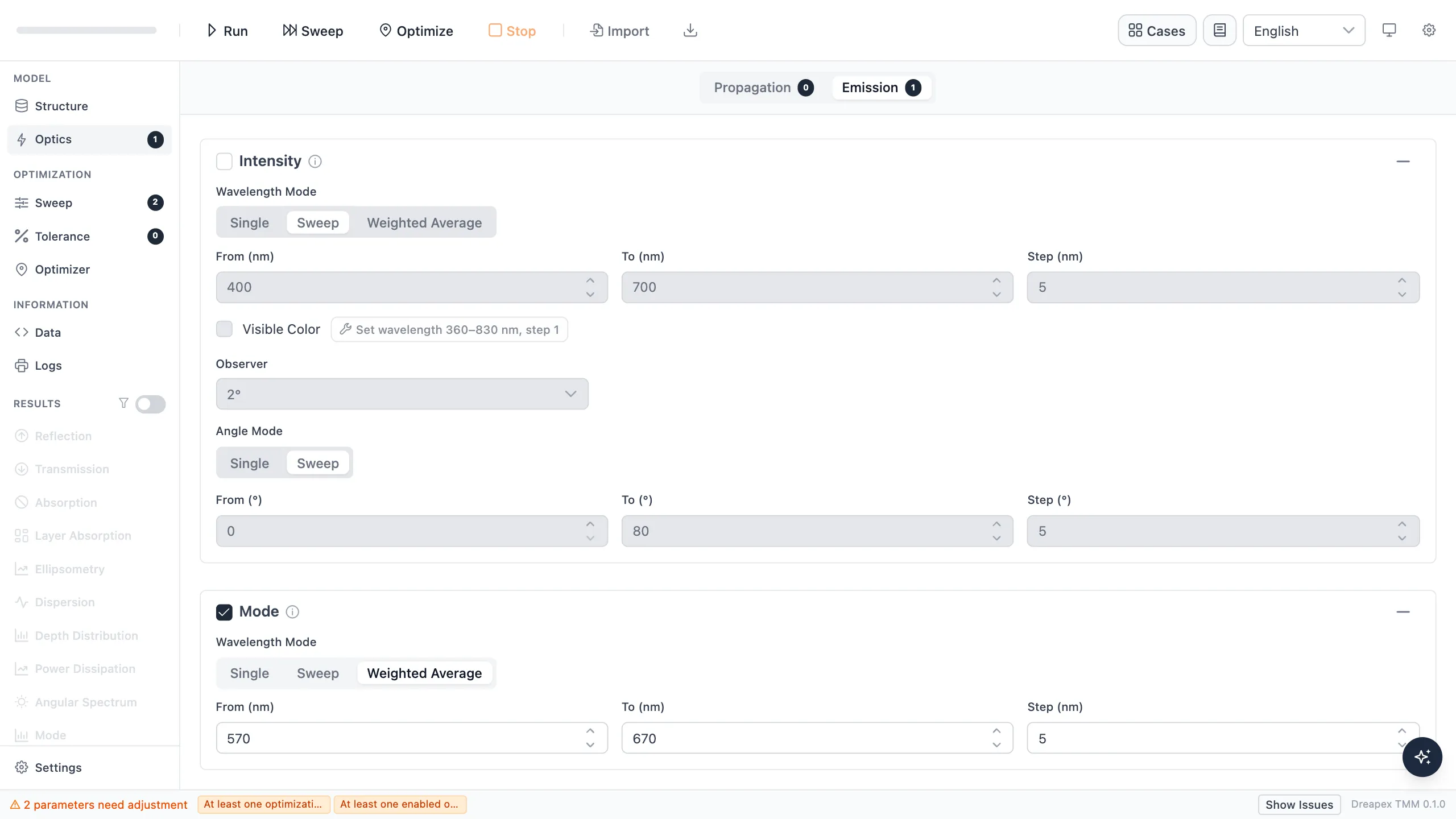
Change the emitter Quantum Efficiency from 1 to 0.9059. On the Emission page under Optics, enable only Mode; set Wavelength Mode to Weighted Average, then set From, To, and Step to 570, 670, and 5 nm. The software weights the result at each wavelength by the imported Red QD PL spectrum.
When Quantum Efficiency is below 1, the optical-channel fractions reported by Mode already include the effective radiative quantum efficiency in the cavity, and the remainder is reported as Non-radiative. The Top Outcoupling value in this sweep therefore corresponds to ηrad,cav × ηout = EQE/γ in Equation (1) of the paper, where ηrad,cav is the effective radiative quantum efficiency in the cavity and ηout is the OCE; it is not ηout alone. To obtain the pure top-outcoupling fraction, divide Top Outcoupling by the sum of all optical channels; for one emitter, that sum equals 1 − Non-radiative.
The spectrum-weighted Mode settings are shown below:
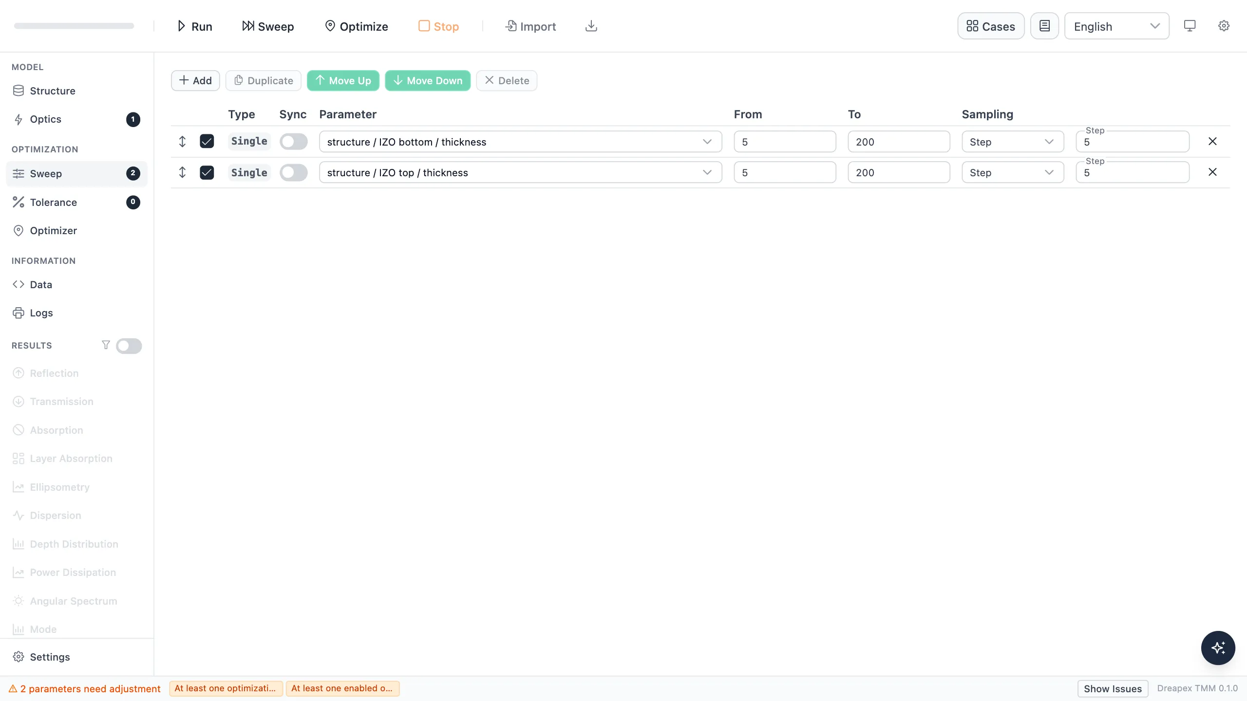
Open Sweep and add two variables of type Single. Set the first Parameter to structure / IZO bottom / thickness and the second to structure / IZO top / thickness. For both rows, set From to 5 nm, To to 200 nm, Sampling to Step, and Step to 5 nm. Enable both rows to obtain 40 × 40 = 1600 thickness combinations.
Sweep result
Section titled “Sweep result”Click Sweep in the toolbar. When the calculation finishes, open Mode and Distribution, set Chart Type to Heatmap, and set Mode channel to Top Outcoupling. The horizontal axis is the bottom-IZO thickness and the vertical axis is the top-IZO thickness. Compare this heatmap with paper Figure 1d:
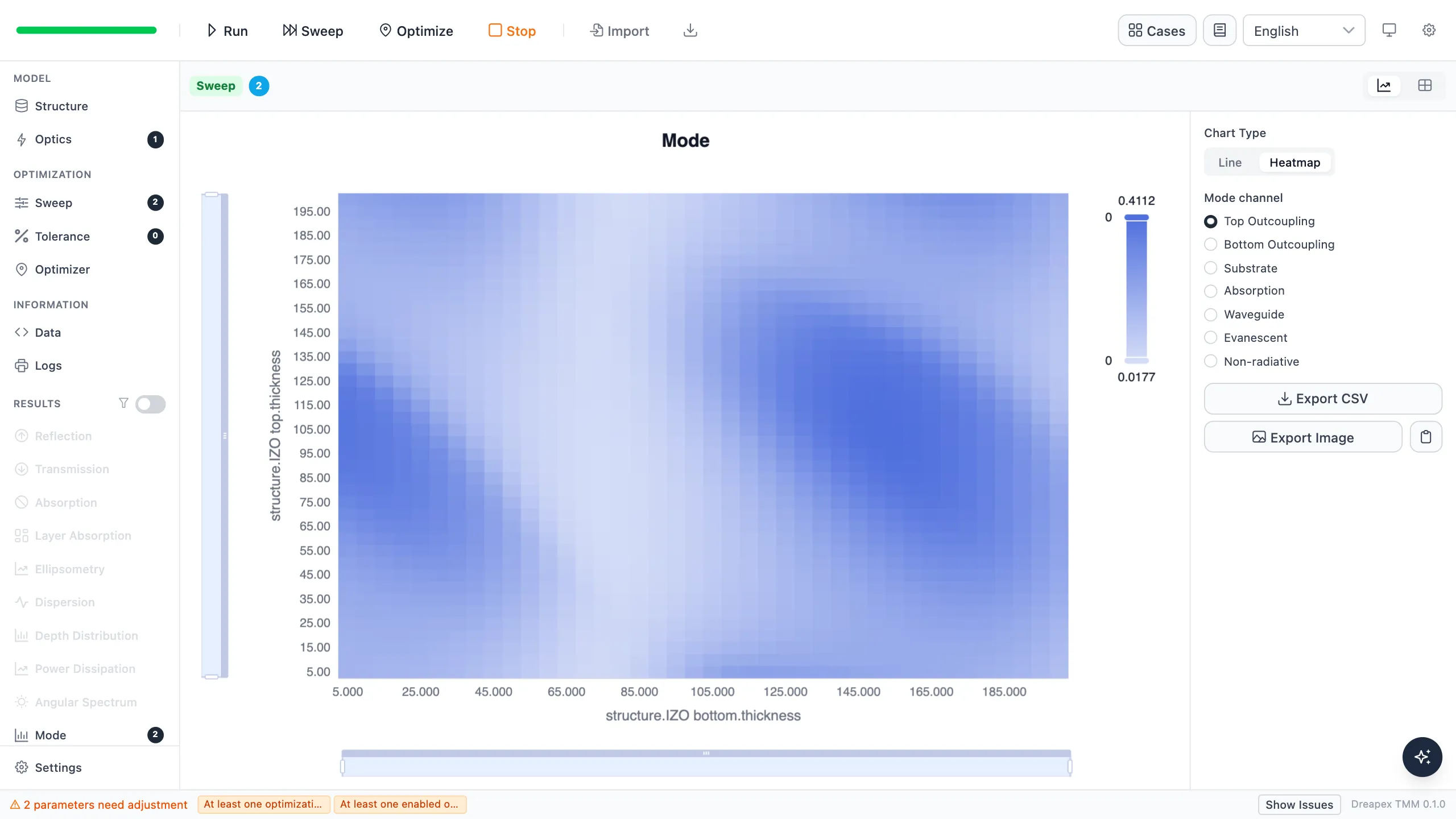
The paper design and the simulated maximum lie in the same high-efficiency region, with top IZO thicknesses differing by one sweep step.
| Quantity | Paper | Simulation |
|---|---|---|
| Optimum bottom IZO | 150 nm | 150 nm |
| Optimum top IZO | 100 nm | 105 nm |
| Peak EQE/γ | 41.4% | 41.12% |
| Simulation at 150/100 nm | Not reported | 40.88% |
The peak metric differs by 0.28 percentage point.
Independent Effects of the Two IZO Layers (Figures 3c and 3f)
Section titled “Independent Effects of the Two IZO Layers (Figures 3c and 3f)”Figure 3c fixes the top IZO at 20 nm and sweeps the bottom IZO. Figure 3f fixes the bottom IZO at 160 nm and sweeps the top IZO. Both calculations use the PL-weighted Mode settings from Figure 1d and an emitter quantum efficiency of 0.9059.
| Target | Fixed thickness | Swept thickness | Step |
|---|---|---|---|
| Figure 3c | IZO top = 20 nm | IZO bottom = 5–200 nm | 5 nm |
| Figure 3f | IZO bottom = 160 nm | IZO top = 5–200 nm | 5 nm |
The published curves include 0 nm. Dreapex TMM requires a positive layer thickness, so the 0 nm points are obtained from separate runs with the corresponding IZO layer removed. An invalid zero-thickness layer is not used.
Bottom-IZO Thickness and Outcoupling Efficiency (Figure 3c)
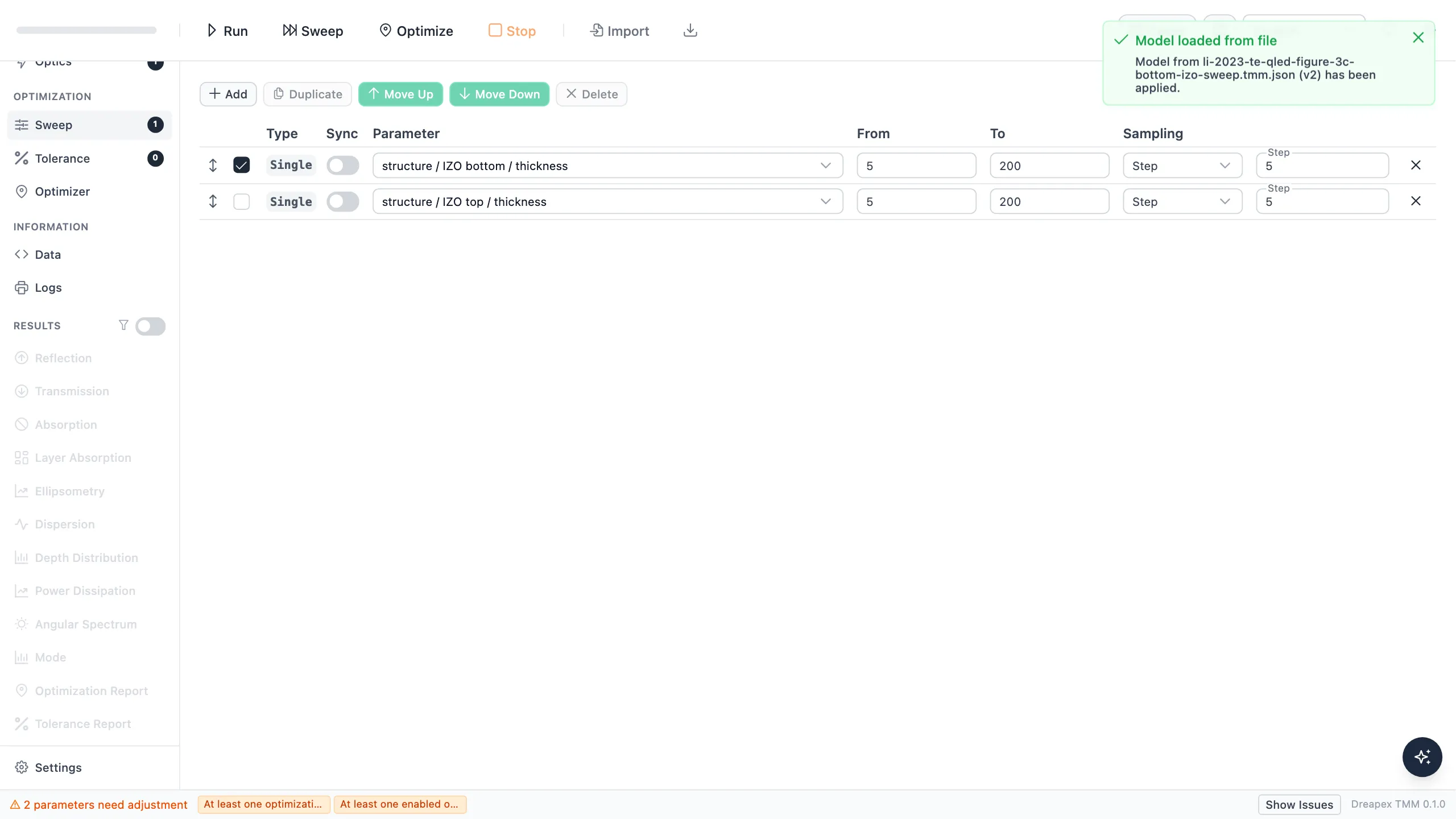
Section titled “Bottom-IZO Thickness and Outcoupling Efficiency (Figure 3c)”Set IZO top to 20 nm. Keep Mode at Weighted Average from 570 to 670 nm with a 5 nm step, and keep the emitter Quantum Efficiency at 0.9059. Retain both thickness rows in Sweep, but enable only structure / IZO bottom / thickness. Set this row to 5–200 nm, set Sampling to Step, and set Step to 5 nm. Disable the top-IZO sweep row.
Click Sweep. When the run finishes, open Mode and Distribution, then set Chart Type to Line. Top Outcoupling is the channel compared with the simulated EQE/γ in the paper; the other channels show where the corresponding power is transferred.
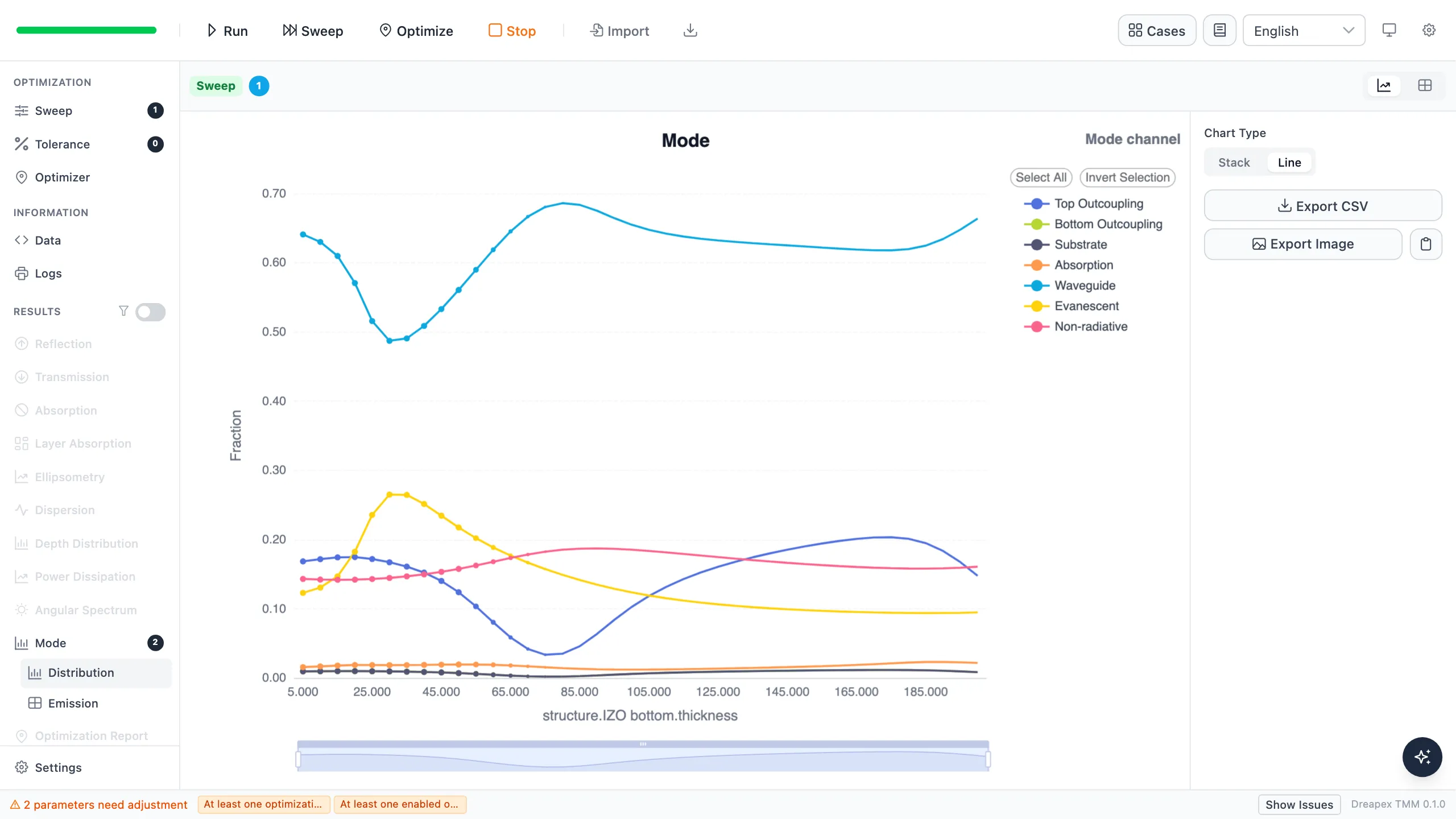
The simulated curve has local maxima at 20 and 175 nm and a minimum at 75 nm. Paper Figure 3c places the two high regions near 20 and 175 nm and the minimum near 80 nm, giving the same sequence of features.
| Simulated position | EQE/γ |
|---|---|
| 20 nm | 17.89% |
| 75 nm | 3.43% |
| 160 nm | 20.27% |
| 175 nm | 20.83% |
The paper reports a maximum experimental EQE of 22.7% for the 160 nm device. That experimental point also depends on charge balance and fabrication differences; this case reproduces only the EQE/γ curve from the optical model.
Top-IZO Thickness and Outcoupling Efficiency (Figure 3f)
Section titled “Top-IZO Thickness and Outcoupling Efficiency (Figure 3f)”Set IZO bottom to 160 nm and keep the same emitter and spectrum-weighted Mode settings. In Sweep, disable structure / IZO bottom / thickness and enable structure / IZO top / thickness. Set the top-IZO range to 5–200 nm, Sampling to Step, and Step to 5 nm.
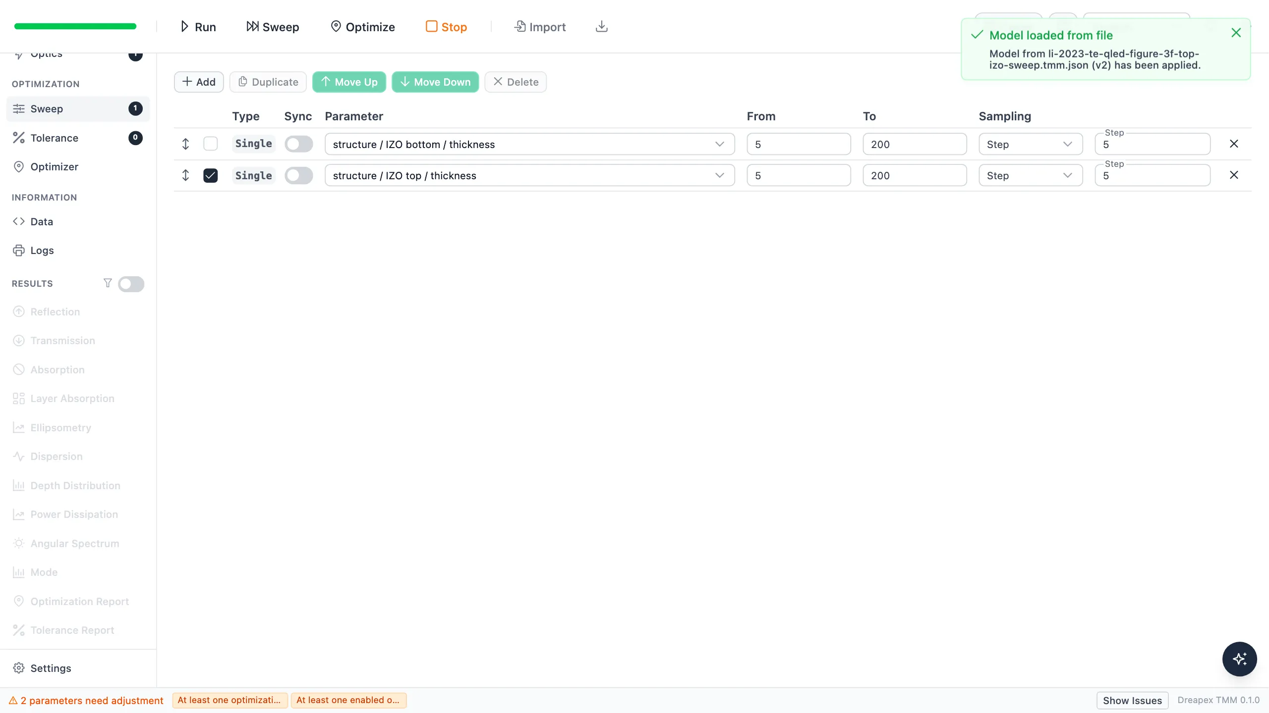
Click Sweep, then select Line in the Mode Distribution result. The result is shown below:
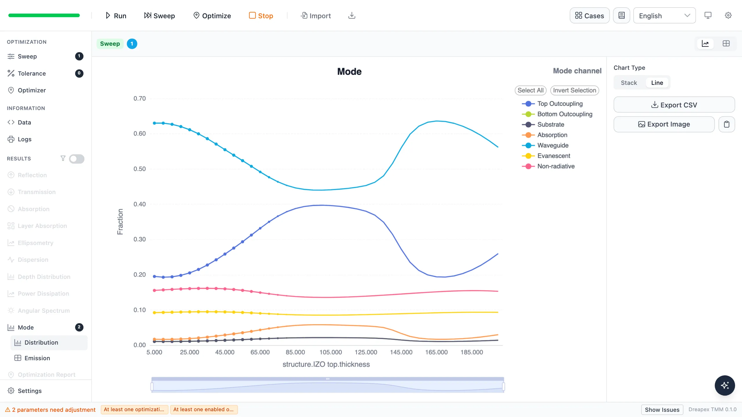
The simulation reaches its only maximum at 100 nm, with an EQE/γ of 40.63%, matching the peak thickness in paper Figure 3f. The simulated values at 20 and 170 nm are 20.27% and 19.78%, respectively, so the curve rises from a low value to the 100 nm peak and then falls again. The paper reports an experimental EQE of 39.2% for the 100 nm device; the experimental points are not simulation outputs from this case.
Effect of Bottom IZO on Mode Partition (Figure 4a)
Section titled “Effect of Bottom IZO on Mode Partition (Figure 4a)”Figure 4a fixes IZO top at 100 nm and sweeps IZO bottom. Set IZO top to 100 nm and change the emitter Quantum Efficiency to 1 so that the optical channels sum to 100%. Keep Mode at Weighted Average from 570 to 670 nm with a 5 nm step. In Sweep, enable only structure / IZO bottom / thickness; set the range to 5–200 nm, set Sampling to Step, and set Step to 5 nm.
Click Sweep. When the run finishes, open Mode and Distribution, then set Chart Type to Stack. The stacked chart shows how power is redistributed among the modes as bottom-IZO thickness changes:
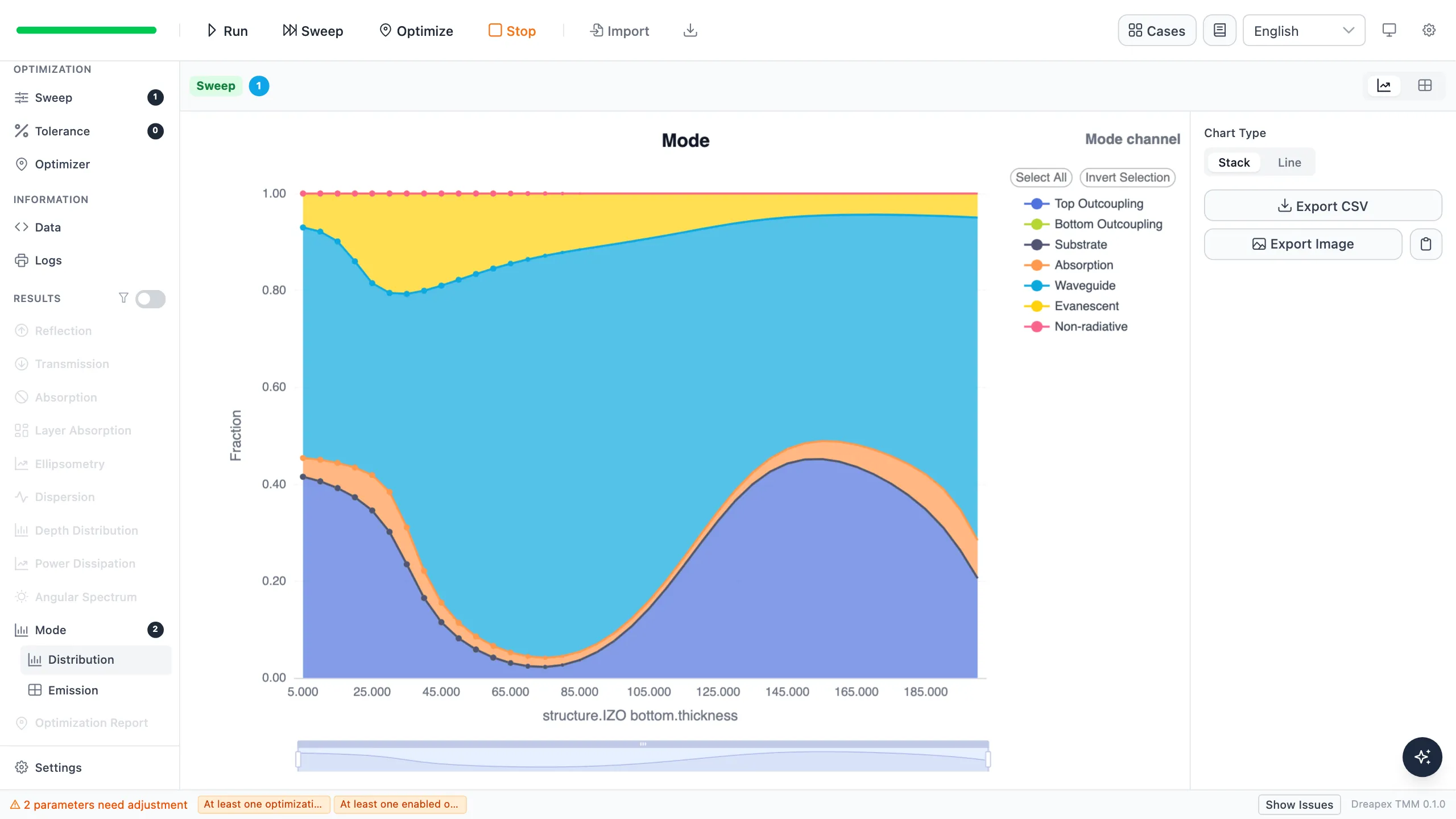
The software screenshot covers the 5–200 nm sweep. A separate run with IZO bottom removed supplies the 0 nm point. The second outcoupling maximum is at 155 nm, one sweep step from the 160 nm value reported in the paper. Waveguide is 46.81% at 160 nm, consistent with the paper’s description of a value close to 50%.
| Bottom IZO | Top Outcoupling |
Waveguide |
Evanescent |
Absorption |
|---|---|---|---|---|
| 0 nm | 41.95% | 47.93% | 6.70% | 3.41% |
| 155 nm | 45.17% | 46.58% | 4.52% | 3.72% |
| 160 nm | 44.63% | 46.81% | 4.42% | 4.12% |
The difference between the paper’s SPP values and Dreapex TMM’s Evanescent values may result from different in-plane-wavevector ranges. From 0 to 160 nm, the reduction in Evanescent follows the trend discussed for SPP in the paper.
Bottom-IZO Thickness and Mode-Peak Positions (Figure 4c)
Section titled “Bottom-IZO Thickness and Mode-Peak Positions (Figure 4c)”Fix IZO top at 100 nm and build separate models with IZO bottom at 0, 5, and 160 nm. Remove the IZO bottom layer for the 0 nm model; do not enter a zero thickness. Enable only Power Dissipation in each model and use the settings below:
| UI field | Setting |
|---|---|
Wavelength Mode |
Single |
Wavelength |
628 nm |
In-plane Vector Type |
In-plane u |
From |
0 |
To |
2 |
Step |
0.002 |
The Figure 4 caption specifies 628 nm, while the Figure 4c horizontal-axis label says 626 nm. This page uses the caption value of 628 nm for the main result and repeats the calculation at 626 nm as a check. The main peak positions differ by no more than 0.004 between the two wavelengths.
Click Run for each model. In each Power Dissipation result, set Polarization and Direction to Total, then click Export CSV. Plot the uInplane and K_total columns from all three files on one logarithmic vertical axis with Matplotlib. Divide every curve by the mean K_total of the 0 nm curve over $0.02 \leq u \leq 0.25$ so that the relative amplitudes remain comparable. The chart contains only real results from this case and does not include a curve taken from the paper.
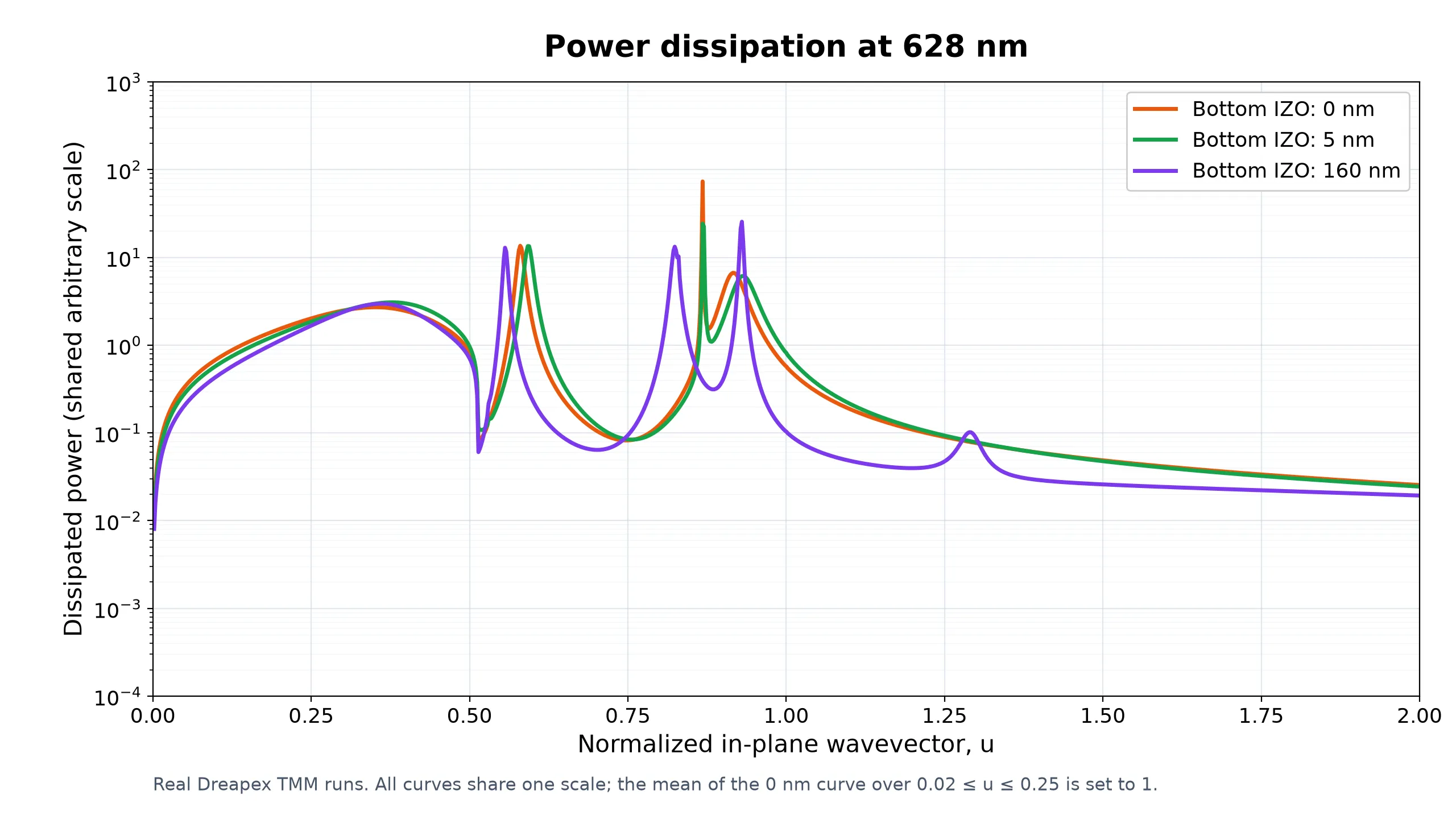
| Bottom IZO | Main peak positions at 628 nm |
|---|---|
| 0 nm | 0.580, 0.868, 0.916 |
| 5 nm | 0.592, 0.868, 0.932 |
| 160 nm | 0.556, 0.824, 0.930 |
The 160 nm curve also has a weak shoulder near 1.29. The main peak pattern and shift directions agree with paper Figure 4c.
Deviation Notes
Section titled “Deviation Notes”- The paper does not provide the original numerical optical-constant files. This case uses data extracted from Supporting Information Figure S1 and linearly interpolated; digitization and interpolation errors affect the cavity phase.
- The two-dimensional thickness sweep uses a 5 nm step, which limits the resolution of the optimum thickness.
- The optimum
IZO topthickness from this case is 5 nm higher than the paper value, and the peak EQE/γ is 0.28 percentage points lower.
Going further
Section titled “Going further”These tutorials cover the operating steps only. The physics behind them, the full parameter reference for each feature, how to read the results, and the algorithm validation all live on the documentation site:
- Transfer-Matrix Method — the physics and formulas behind these tutorials
- Feature Guide — complete reference for every screen and parameter
- Results — how to read each kind of output
- Open Dreapex TMM — build and simulate in the browser